
Spark core datasheet
Subsystems
Microcontroller
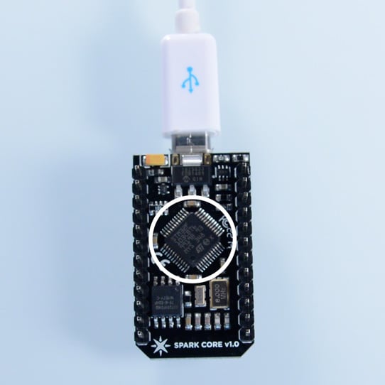
Spark Core v1.0 uses the STM32F103CB - ARM 32-bit Cortex M3 based - microcontroller for its brain power. You can download the datasheet here.
Some of its key features are as follows:
- ARM 32-bit Cortex™-M3 CPU Core
- 72Mhz operating frequency, 1.25 DMIPS/MHz (Dhrystone 2.1)
- 128KB of Flash memory
- 20KB of SRAM
- 12 bit ADC
- USB 2.0 full-speed interface
- USART, SPI and I2C interfaces
- JTAG Debug mode
Wi-Fi module
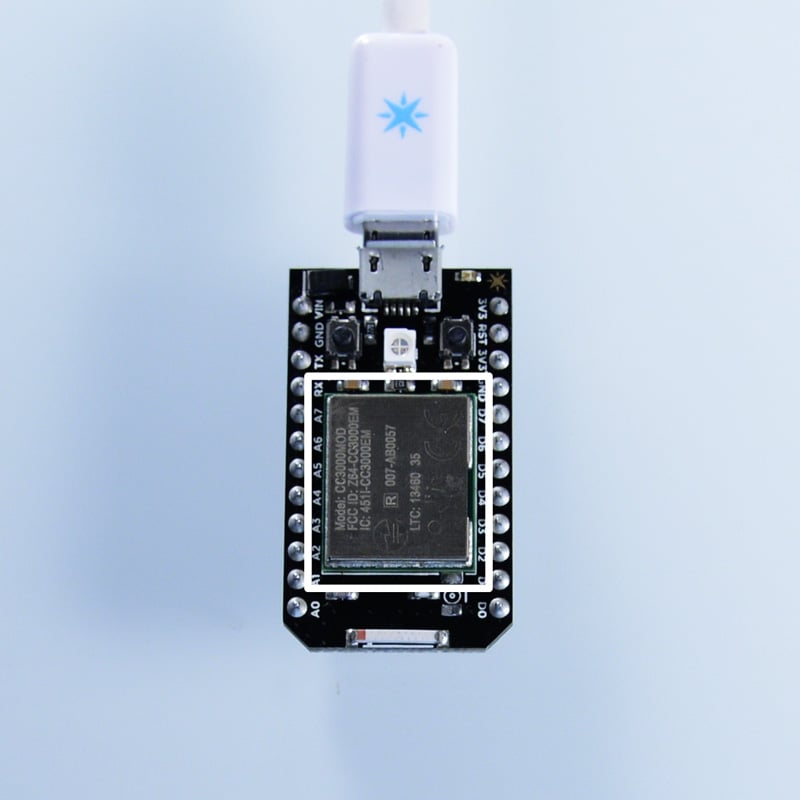
Core v1.0 uses TI's CC3000 module for the Wi-Fi communications.
Some of the key features of the CC3000 module are as follows:
- IEEE 802.11 b/g compliant
- Radio Performance
- TX power: +18.0 dBm at 11 Mbps, CCK
- RX sensitivity: – 88 dBm, 8% PER, 11 Mbps
- Operating temperature: – 20° C to 70° C
- Wireless security subsystem
- WEP
- WPA Personal
- WPA2 Personal
- FCC, IC, and CE certified with a chip antenna
- SPI host interface
External flash
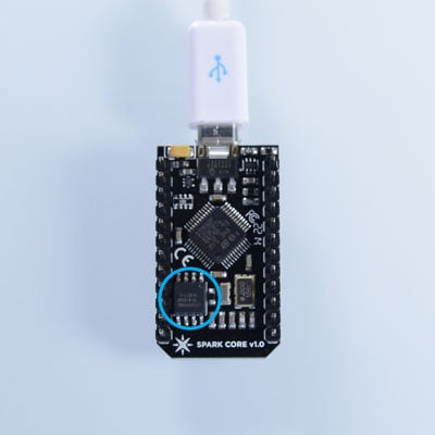
In addition to having 128KB of internal flash memory for storing the firmware, the Core also features an external SPI based flash memory chip - SST25VF016B. This memory space (a total of 2MB) is used to store the factory reset firmware, a back up firmware, a copy of the firmware sent during Over The Air (OTA) update and the keys. Part of the space is also available to the user who can use it to store log data, user parameters, etc. A detailed description of the memory mapping can be found further down this document in the memory mapping section.
Since the flash memory is non-volatile, it retains the data even after turning off the power. According to the manufacturer of the chip, the data retention of this memory is greater than 100 years, which we reckon should be good enough for now. Also, note that the maximum read-write endurance is limited to 100,000 cycles. meh.
Power regulator
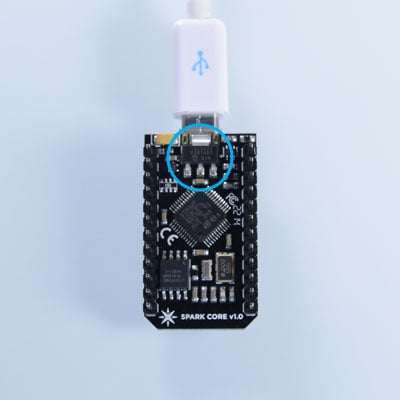
The entire Core, including all of the on board peripherals run at 3.3V DC. So, in order to power the Core from the USB port or an external power supply, we need to downconvert the voltage before feeding it into the Core. We went through a couple of iterations before choosing Microchip's MCP1825S-3302E power regulator which comfortably meets the specs.
Some of its key features are:
- 500mA output current
- Input voltage range of 3.6 to 6.0V (for 3.3V output)
- Low Dropout (LDO) voltage of 210mV at 500mA
- SOT-223 package that sits nicely on the other side of the USB connector. The connector also acts as an additional heat sink.
- Short Circuit Current Limiting and Over Temperature Protection
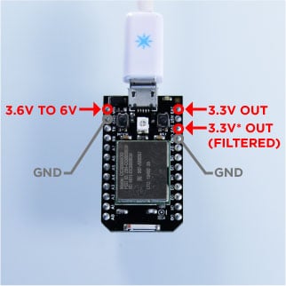
This means, you can power the Core via the USB port or via the VIN pin from an external power supply that can range from 3.6V to 6.0V DC. Ideal sources of power can be: 3.6V LiPo battery, 4AA battery pack, backup USB battery or an USB wall charger.
RF circuit
The RF circuit is probably where we spent the most time on during hardware design. RF design is like voodoo black magic, so we sought guidance from the industry experts before finalizing the component values and placement.
You can download a copy of the RF test report here.
Pins and I/O
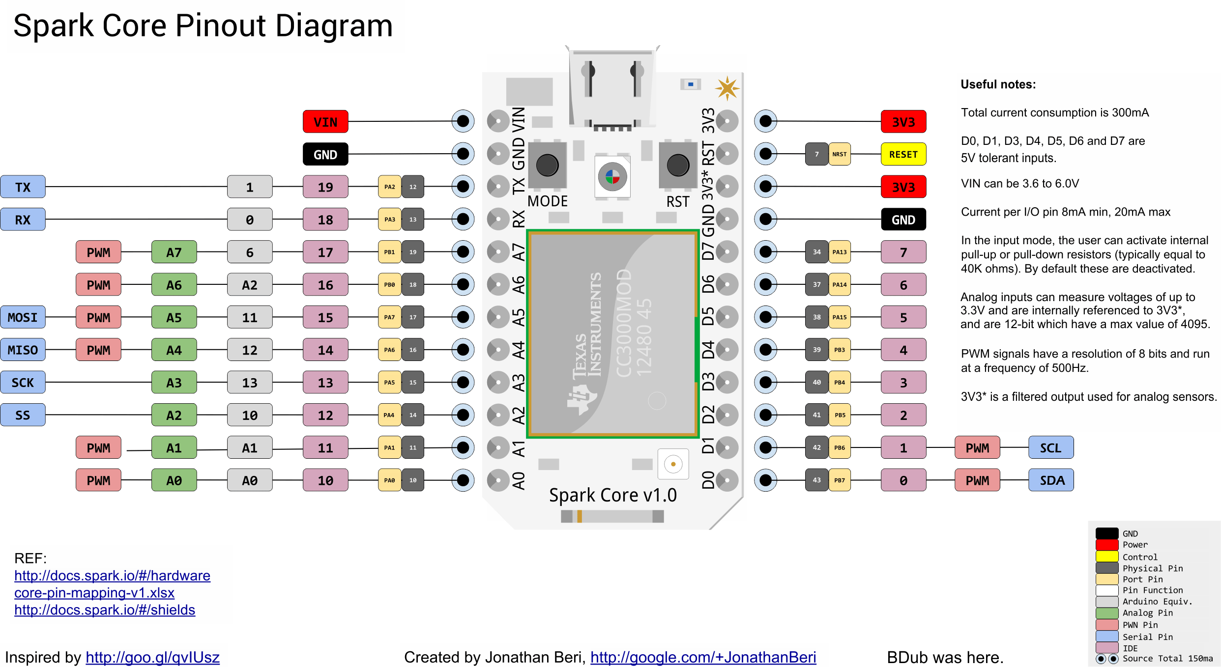
The Spark Core offers a total 18 I/O pins to the user: D0 to D7, A0 to A7 and two pins that are preset to serial - TX and RX. All of these I/O pins run at 3.3V and the user should keep this in mind before attaching any external peripherals to them. The only exception to this are the following pins that are tolerant to 5V inputs:
D0, D1, D3, D4, D5, D6 and D7
Click here to view a larger pinout diagram
Digital pins
Each pin on the Core can either be configured as input (with or without pull-up or pull-down) or as output (push-pull or open-drain) using the pinMode() function.
After setting them up, the user can then write to or read from the pins using digitalWrite() and digitalRead() functions respectively.
Each of these pins can individually source/sink a maximum of 20mA. In the input mode, the user can activate internal pull-up or pull-down resistors (typically equal to 40K ohms). By default these are deactivated.
Analog inputs
Pins A0 to A7 can be set up as analog inputs and can measure voltages of up to 3.3V and are internally referenced to VDD. The user can read the pins using analogRead() function which returns a 12bit value.
Analog outputs
This term is misleading and misused but is widely adopted in the Arduino community. The pins that are set to output an analog value don't actually output an analog voltage but rather produce a PWM signal whose duty cycle can be varied thus varying the total average power of the signal. On the Core, the PWM signals have a resolution of 8 bits and run at a frequency of 500Hz.
Having said that, the user can send analog values to the pins using the function analogWrite().
This feature is only available on the following pins: A0, A1, A4, A5, A6, A7, D0 and D1.
Serial (UART)
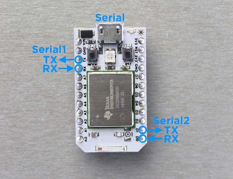
The Core features three serial ports. The first one is a CDC (Communications Device Class) available over the USB port. When configured, it will show up as a virtual COM port on the computer. (usage: Serial.begin(9600);)
The second one is a hardware USART available via the TX and RX pins on the Core. (usage: Serial1.begin(9600);)
The third one is a hardware USART available via the D1(Tx) and D0(Rx) pins on the Core. (usage: Serial2.begin(9600);)
Configuration and use of all of these serial ports is described in the serial functions.
NOTE: Please take into account that the voltage levels on these pins runs at 0V to 3.3V and should not be connected directly to a computer's RS232 serial port which operates at +/- 12V and can damage the Core.
SPI
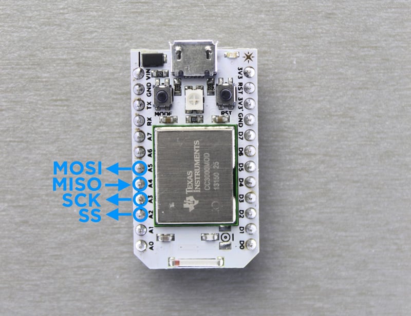
The Serial Peripheral Interface is available on pins:
A2: SS (Slave Select)A3: SCK (Serial Clock)A4: MISO (Master In Slave Out)A5: MOSI (Master Out Slave In)
NOTE: All of these pins run at 3.3V logic levels.
I2C
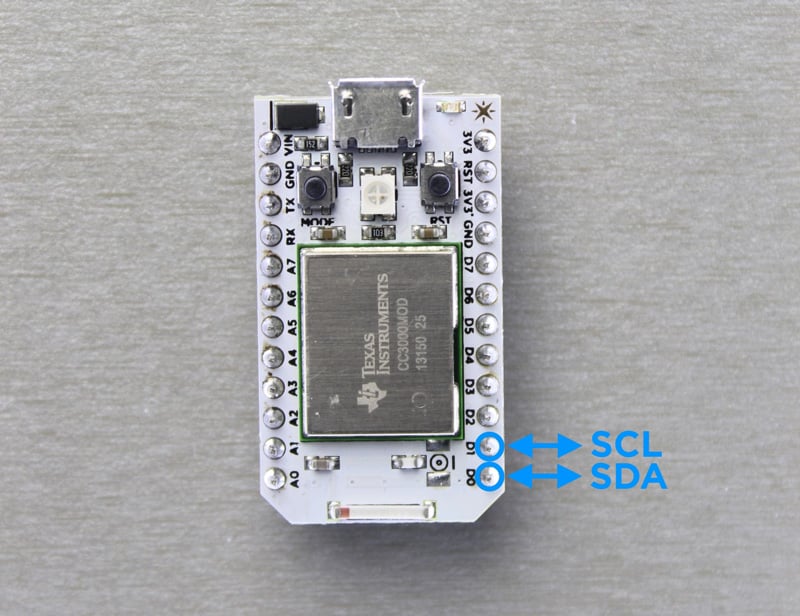
I2C communication pins are multiplexed with the standard GPIO pins D0 and D1.
D0: SDA (Serial Data Line)D1: SCL (Serial Clock)
Both of these pins run at 3.3V logic level but are tolerant to 5V inputs.
JTAG
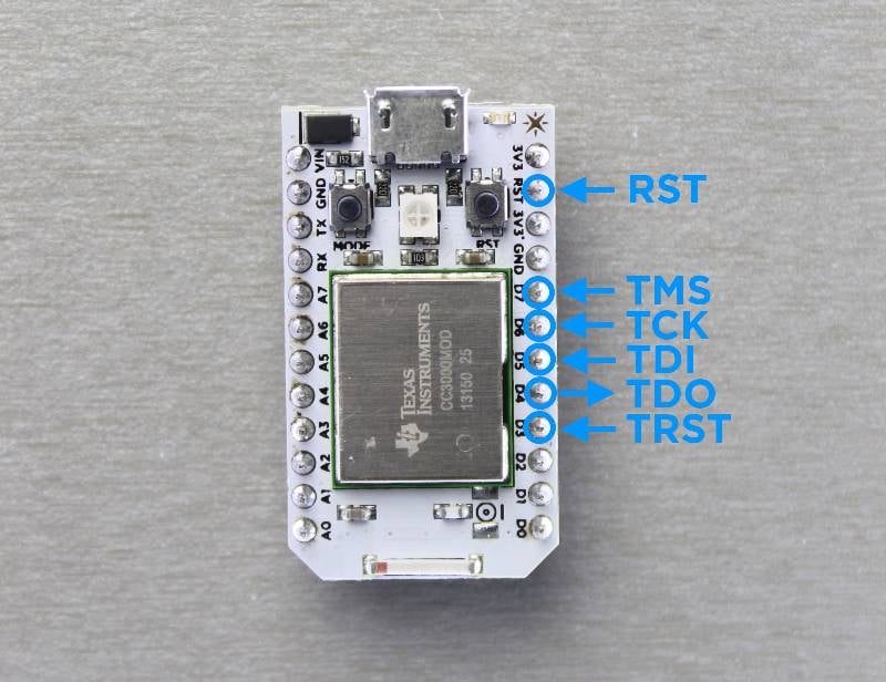
In addition to having the ability to load new firmware over USB and Wi-Fi, the users also have direct access to the STM32 chip via the JTAG channel. In order to do this, you will need a JTAG shield and a JTAG programmer. You could make your own JTAG shield or buy one from us. Currently we have only tested the ST-LINK/V2 programmer successfully.
The hardware files for the JTAG shield are available here.
Memory mapping
Internal flash memory map
The STM32 has a total of 128KB internal flash memory which is divided into three main regions by us. Beginning at the top of the memory space is where the bootloader is saved and locked. The second region is reserved for storing system flags and the third region holds the actual user firmware.
| Memory Address | Content | Size |
|---|---|---|
| 0x08000000 | Bootloader | 19 KB max |
| 0x08004C00 | System Flags | 1 KB max |
| 0x08005000 | Core Firmware Location | 108 KB max |
External flash memory map
The external flash memory gives us an additional 2MB of storage space. This space is used to store the public and private keys, the factory reset firmware, a back-up firmware and a copy of the firmware sent Over The Air (OTA). The rest of the memory space is available to the user.
| Memory Address | Content | Size |
|---|---|---|
| 0x00000 | Reserved | 4KB |
| 0x01000 | Public Key | 294 Bytes - 4KB max |
| 0x02000 | Private Key | 612 Bytes |
| 0x20000 | Factory Reset Firmware Location | 128 KB max |
| 0x40000 | BackUp Firmware Location | 128 KB max |
| 0x60000 | OTA Firmware Location | 128 KB max |
| 0x80000 | End of OTA Firmware | |
| NOT USED | ||
| 0x200000 | End of Flash Memory |
Electrical characteristics
Power
| Parameter | Min | Max |
|---|---|---|
| Input Voltage (at VIN) | 3.6 V | 6.0 V |
| Total Current Consumption | 50mA | 300mA |
| Current Consumption in Deep Sleep | 3.2 μA | - |
| Current per I/O pin | 8mA | 20mA |
RF
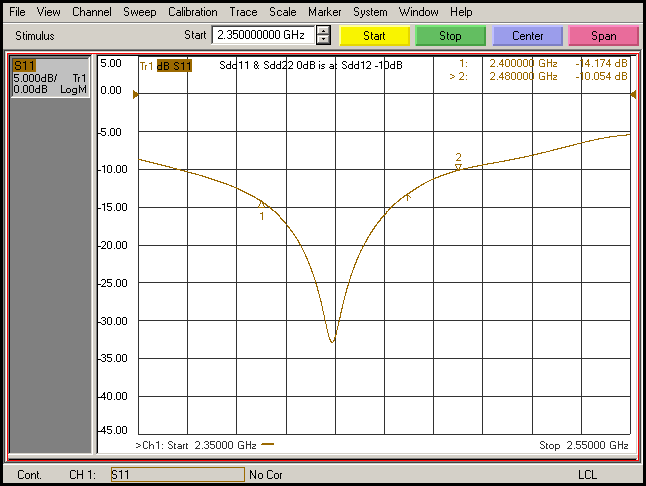
With the on board chip antenna, the peak return loss (S11) has been measured and verified to be in the excess of 20dB.
The transmission loss for the U.FL connector has been measured to be approximately 0.5 to 0.75dB.
Types of Cores
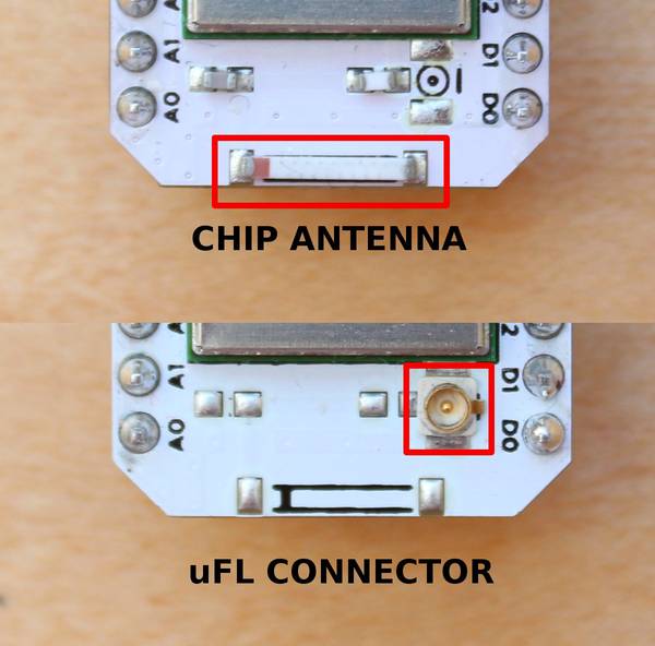
Currently the Core is available in two flavors. With an on-board chip antenna or an uFL connector to connect an external antenna.
Chip antenna
This version of the Core comes with an on board chip antenna that gives a signal strength similar to a mobile phone. In most cases, a simple plastic enclosure will not affect the signal strength of the chip antenna.
uFL Connector
If you want to improve the signal strength of the Core, you can connect an external antenna with the help of the uFL connector. Most antennas that are designed to operate at 2.4GHz or are Wi-Fi rated will do the job. You can also make your own cantenna!
Physical layout
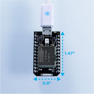
The header pins on the Core are spaced at an interval of 0.1", which is the standard pitch size for proto-boards and breadboards. The physical layout of the Core was inspired from the Arduino Pro Mini board.
A Core part for EAGLE can be found in the Particle EAGLE library
Mechanical drawings of the Core are available here.
| Parameter | Value (imperial) | Value (metric) |
|---|---|---|
| Length | 1.47" | 37.34 mm |
| Width | 0.8" | 20.32 mm |
| Height | 0.5" | 12.7 mm |
| Weight | 0.49 ounces | 14 grams |
Known errata
We are tracking known errata with this datasheet here. These issues/errors in the datasheet will be resolved in subsequent revisions.