
LCC Module SMT
This document describes the processes of secondary SMT soldering and desoldering of the Particle Asset Tracker SoM device. It is also applicable to other LCC (leadless chip carrier) devices such as the E-Series.
Modules
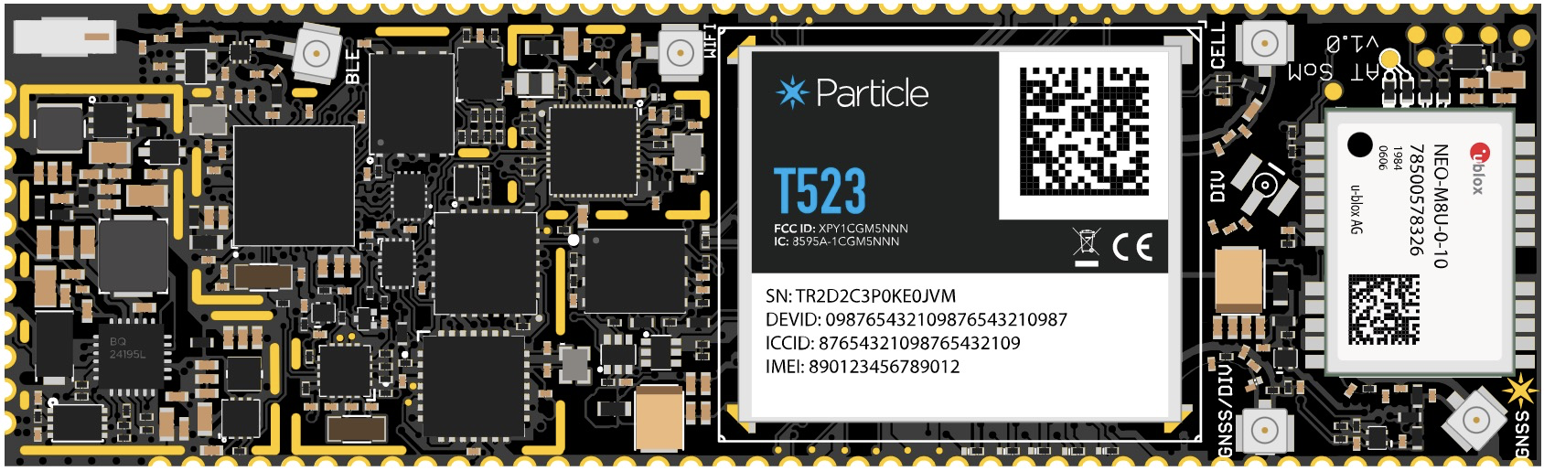
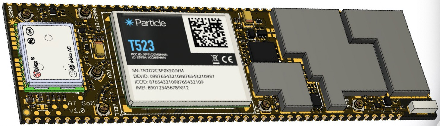
Asset Tracker SoM
Packing methods
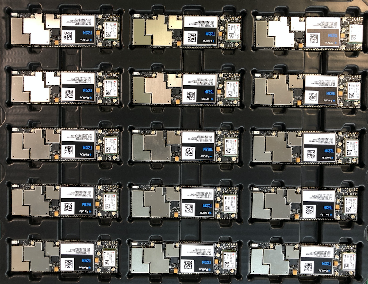
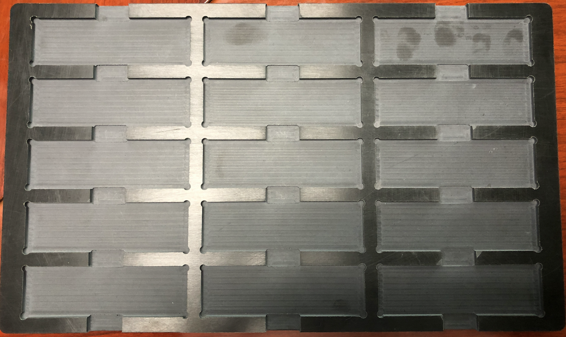
Particle provides MBB (Moisture Barrier Bag) in packing trays:
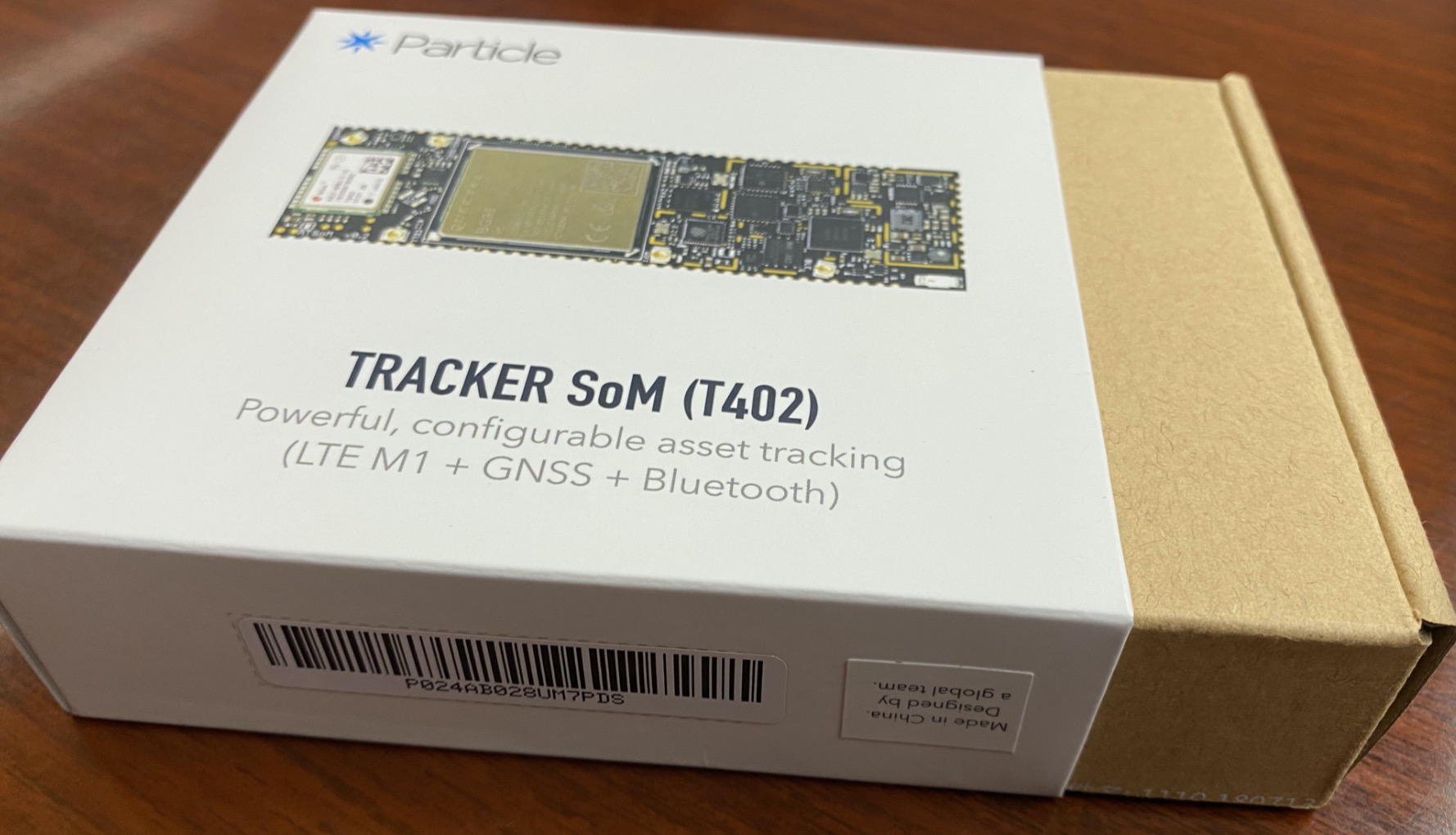
And small gift boxes:
Requirements for SMT
Chip mounter
Feeder: Supports auto tray feeder.
Image processing: Optical plummet centering.
Diameter of nozzle: Select the suitable nozzle according to the module size. The recommended diameter of the nozzle should be not less than 40 % of the module’s shorter side. For example, if the module size is 20.0 mm × 20.0 mm, the nozzle diameter should be 8.0 mm at least.
Soldering requirements
It is recommended to use reflow soldering equipment with eight zones at least.
In a lead-free reflow oven, the real peak temperature at the temperature measuring point of pads at the bottom of modules should be greater than 238 °C, and the temperature of that with SMT carrier is recommended to be 240 °C to 246 °C to avoid cold solder joints. Further, based on the material's heat absorption and size of the carrier, the period in which temperature is over 217 °C should be extended by up to 10 seconds.
If the thickness of the motherboard is less than 1.0 mm, it is recommended to use carriers when soldering to prevent warpage of the motherboard.
For the finishing of pads on the PCB, it is recommended to use the same finishing technique as the module’s pin, that is, ENEG (Electroless Nickel Electroless Gold) or ENIG (Electroless Nickel Immersion Gold). HASL (Hot-Air Solder Leveling) is not recommended.
Requirements for manufacturing
MSL and Moisture-proof requirement
Particle SMD modules are sensitive to moisture. According to IPC-JEDEC standard, the moisture sensitive level (MSL) of Particle SMD modules is rated as “3”. Please make sure the vacuum package (MBB: Moisture Barrier Bag) is intact before using. After opening the package, please confirm the status of the humidity indicator card in the sealed package. To prevent the module from permanent damage, baking before reflow soldering is required if circumstance below occurs:
Humidity indicator card: At least one circular indicator is no longer blue.
Normal:
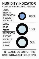
Not blue:
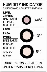
- For those gift box packing, please bake the units more than 8 hrs at 110°C and then do the soldering.
Storage
Recommended Storage Condition: The temperature should be 23 °C ±5 °C and the relative humidity should be 35–60 %.
Storage Life (in sealed vacuum package): 24 months in Recommended Storage Condition.
Floor life and temperature & moisture control
Floor life refers to the allowable time period between removal of the module from a package, dry storage, or dry bake and the solder reflow process. Floor life of MSL-3 products should be 168 hours. In a plant where the temperature is 23 ±5 °C and relative humidity is below 60%, the module must be processed in solder reflow or other high-temperature operations within 168 hours after the package is removed. Otherwise, the module should be stored in an environment where the relative humidity is less than 10 %, such as a dry cabinet.
To avoid blistering, layer separation and other soldering issues, it is forbidden to expose the modules to the air for a long time. It is recommended to start the solder reflow process within 24 hours after the package is removed if the temperature and moisture do not conform to IPC/JEDEC J-STD-033. And do not remove the packages of modules if they are not ready for soldering.
In the case that a violation of moisture-proof requirement or broken vacuum package occurs, or before repairing, baking is required. In this case, the module should be baked for 8 hours at 120 ºC ±5 ºC to avoid blistering, crack and layer separation.
Please take out the module from the package and put it on high-temperature resistant fixtures before baking. All modules must be soldered to PCB within 24 hours after the baking, otherwise put them in the drying oven.
Stencil design requirements
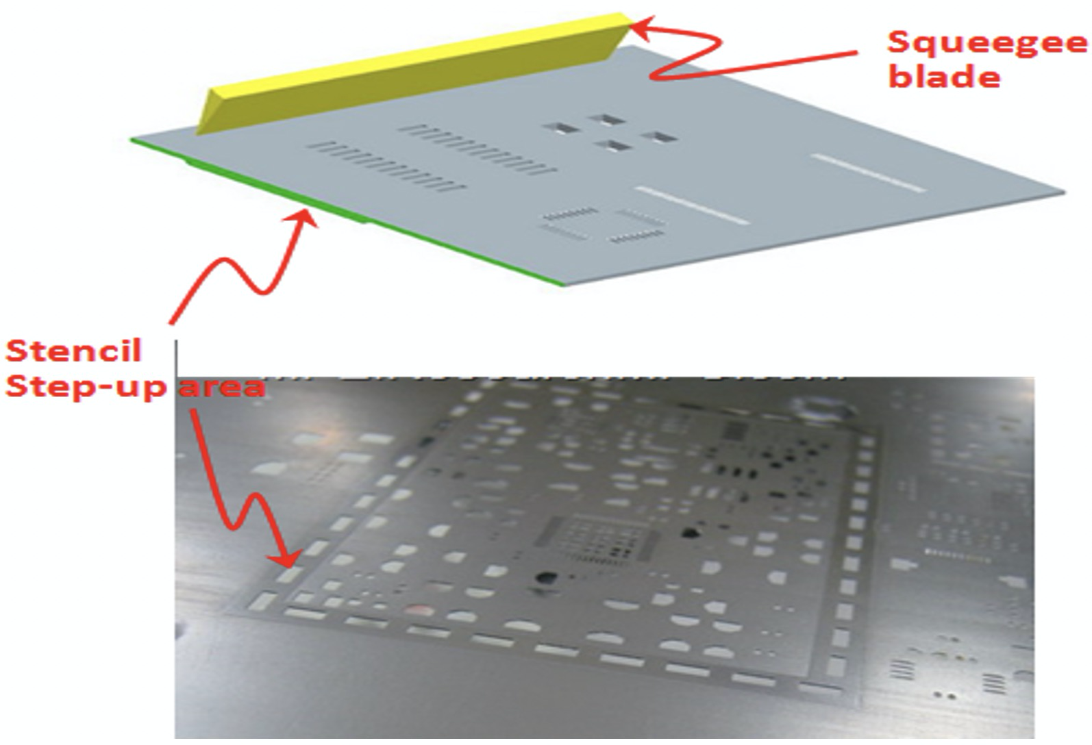
To ensure the solder paste is enough and soldering joints are reliable, we use a Step-stencil for the module:
STEP-UP Stencil and STEP-DOWN Stencil are carried out on the steel sheet to use a single stencil to achieve different thicknesses of solder paste across different areas. According to the performance of components, the size of connection end, and the lands, this type of stencil can accurately control the amount of solder paste applied to the different components and keep the solder paste printing process efficient and accurate.
The stencil thickness of the area for the module should be partly stepped-up on the bottom surface (Touch to the PCB side).
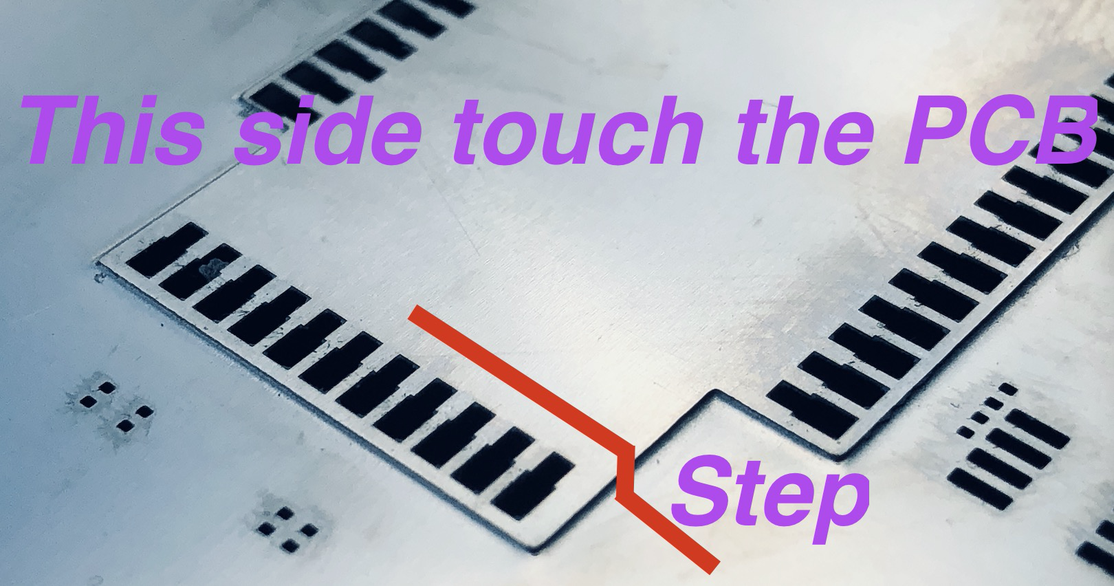
The area in red rectangle in this stencil is 0.30mm, the other area for this stencil is 0.08mm.
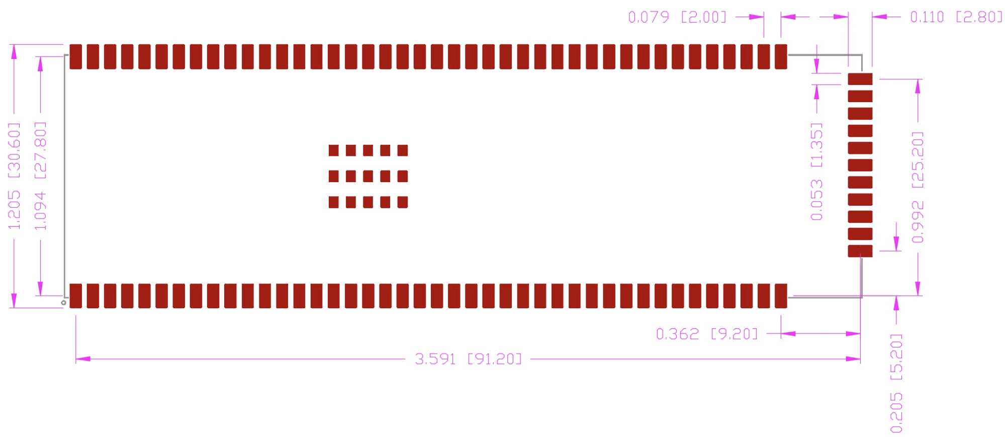
PCB Layout Sample:
All these areas with 0.30mm:
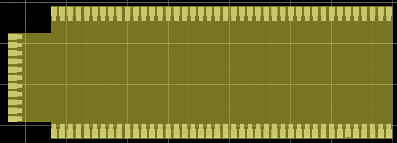
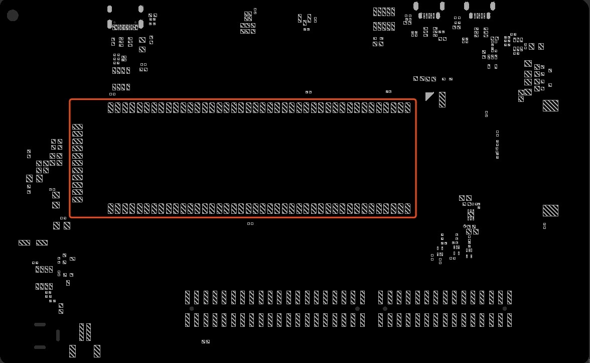
Aperture design for the whole module:
Enlarged view of the pads:

Enlarged view of single pad:
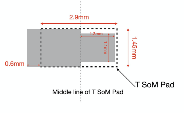
The innermost edge of the aperture for each single pad under the module should be reduced to 1.1 * 1.3mm and the outermost edge should be extended to 0.6mm.
Base board design
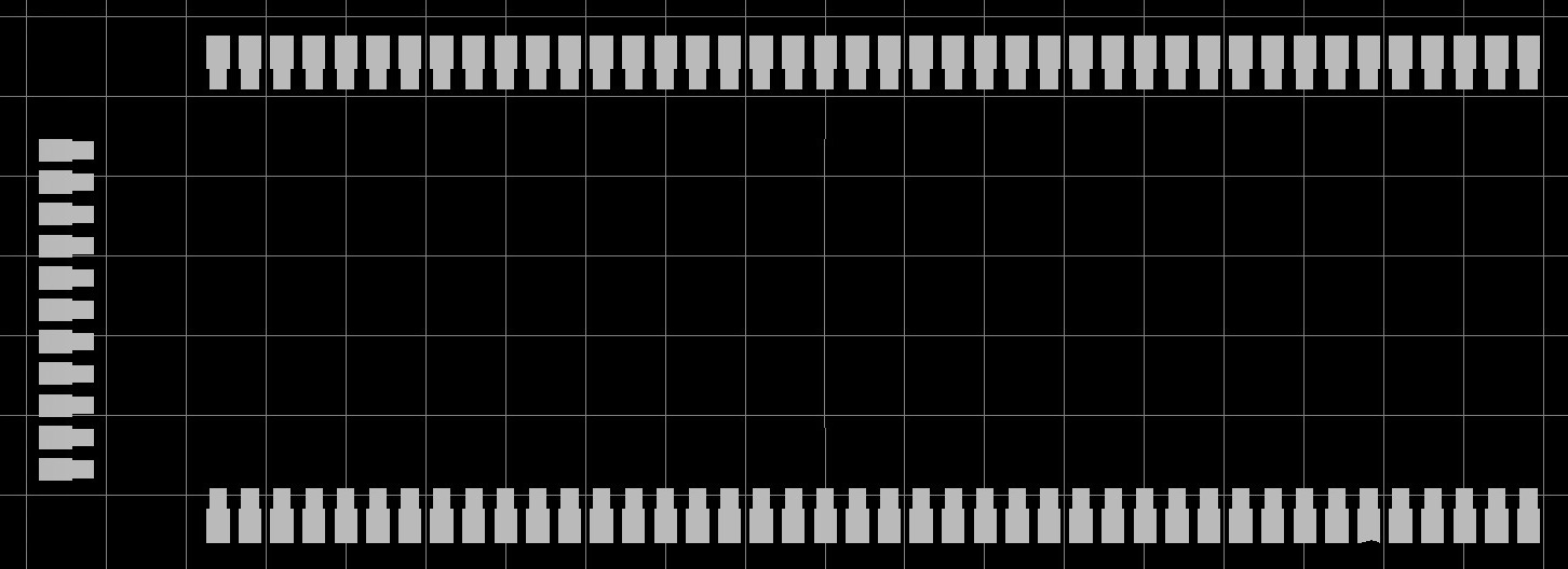
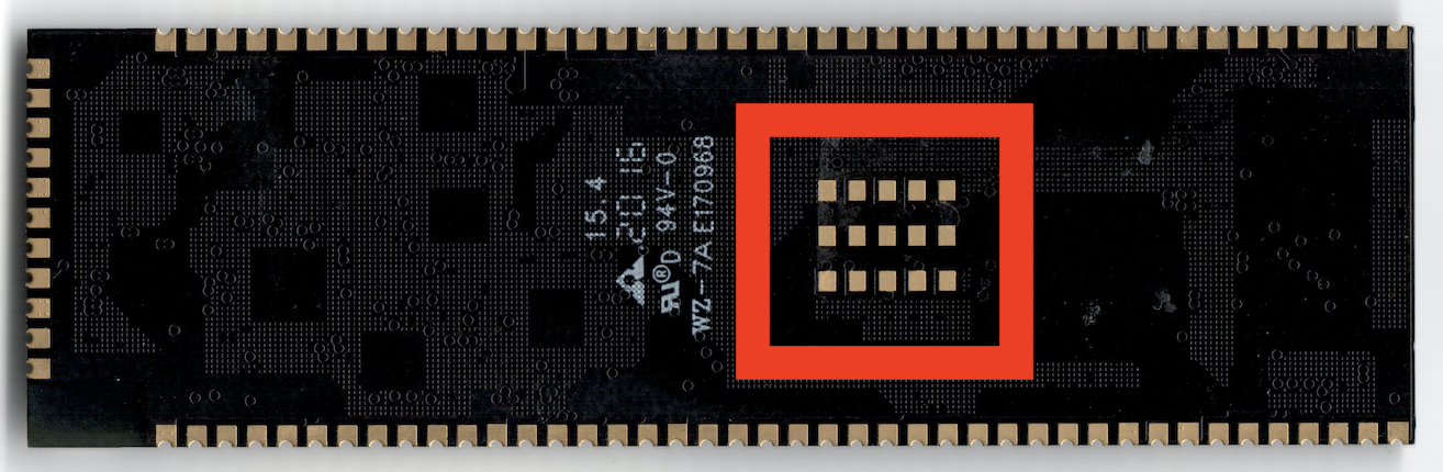
The pads in the center of AT SoM are used for internal R&D testing, and it is recommended to ignore them. There is no need to design stencil apertures to connect these.
There is no need to design stencil apertures for the pads in the center:
Stencil aperture without center pads:
Do not place components within 12.0 mm around the module. Since the stepped area will increase the volume of solder paste, keep away from the stepped-up area to avoid solder bridging and/or short circuits, or please optimize the stencil design depending on the actual situation through DOE.
It is recommended that no component should be mounted in the area at the backside of the module on PCB, for the convenience of heating and repairing.
The following is the design of the recommended pads on the PCB as seen from the component side:
Mounting process
Load materials
In order to ensure mounting accuracy, for single modules that have been unpacked for baking, it is recommended for the customers to use a dedicated tray/fixture for module loading.
Automatic placement
Select a suitable nozzle according to the module size. To keep the module's stability, please ensure that the nozzle is placed in the center of gravity, image detection and recognition are 100 % passed, and keep a medium speed when mounting the module. After the module is placed onto the motherboard, the module pins should be in alignment with the corresponding solder paste on the motherboard’s pads.
Reflow soldering
It is recommended to test the temperature based on real modules. Thermocouple temperature test points should be applied to both pins on four sides and that at the bottom, to guarantee required soldering temperature. Please refer to the recommended ramp-soak-spike thermal profile for lead-free reflow soldering in the following figure.
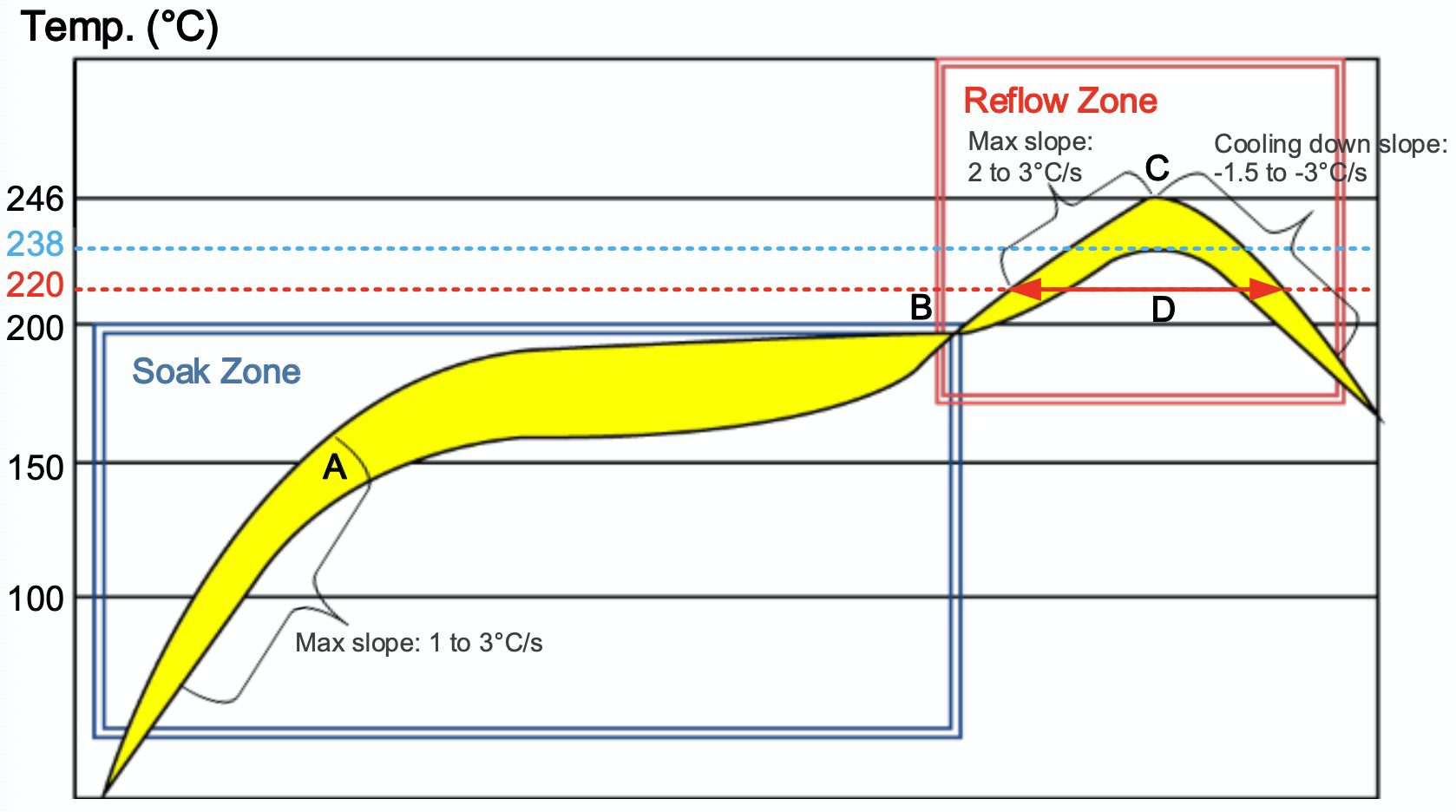
| Factor | Recommendation |
|---|---|
| Soak Zone | |
| Max slope | 1 - 3 °C/s |
| Soak time (between A and B) | 70 - 120 s |
| Reflow Zone | |
| Max slope | 2 - 3 °C/s |
| Reflow time (D: over 220) | 45 - 70 s |
| Peak temperature | 238 °C/s - 246 °C/s |
| Cooling down slope | -1.5 to - 3 °C/s |
| Reflow cycles | |
| Max reflow cycles | 1 |
Temperature
The real soldering temperature is affected by factors such as carrier, solder paste, size and thickness of PCB substrate, thermal durability of components, and the PCB design, etc. If the recommended specifications cannot be reached, please contact Particle technical support, or the module may be damaged during reflow soldering.
Carrier
For motherboard with thickness of less than 1.0 mm, it is recommended to use high Tg material or to use board carrier during reflow soldering, to prevent the motherboard warpage due to heat.
Cooling
By controlling the cooling rate can the soldering defect (fragile solder joint) and negative effects on mechanical stress be avoided. Proper cooling rate will help to make the solder joint lustrous with lower solder fillet. The proper cooling rate should be -3 °C/s.
Visual inspection
Please implement inspections on the soldering quality with X-ray or other optical methods after reflow soldering. For relevant standards, please refer to IPC-A-610G, as this is a BTC package, the bottom pad was soldered is enough, if the solder rises to 25% up the side of the fillet the better.
Desoldering & Resoldering
Please pay attention to the following factors for heating and desoldering:
The motherboard should be baked at 110 °C for 8 hours to prevent damp PCBs from being damaged after direct heating. It is important to ensure that all components on the motherboard stand baking at 110 °C.
Do not disassemble and desolder the module itself, or the warranty will terminate immediately.
Desoldering
Please use a heat gun to heat the solder joints from both sides of the motherboard to remove the module. ESD protection must be implemented during the desoldering.
The temperature of the heat gun should be about 320 °C to 350 °C to release enough heat. The wind speed and distance should be adjusted according to the actual situation.
If the motherboard has been exposed to the air for exceeding 48 hours, then it should be baked before desoldering.
During heating, the motherboard should be laid flat and fixed to avoid movement, and the distance between the motherboard and the nozzle should be from 2.0–3.5 cm.
Move the nozzle along the edge of the module at a constant speed. When all of the solder joints are melted, quickly take off the module along the diagonal direction with tweezers and lay it on a flat cooling platform for cooling.
For the module larger than 30.0 mm × 30.0 mm, a BGA rework station or heat gun (with larger outlet nozzle) can be used to desolder components. To prevent separation between pad and circuit as well as PCB blistering caused by long-time heating on a single side, pre-heating is needed at the bottom side of the module when heat gun is used for desoldering. It is recommended to inspect the soldering quality of modules by X-rays if there are pads in the middle of the module.
If the rework station was used, please make sure the correct desoldering temperature profile was used accordingly. Refer to the suggested SMT reflow profile is required.
Resoldering Procedure
Remove superfluous solder paste on the pads of motherboard with electric soldering iron and keep the pads flat.
Pre-apply solder paste on the pads with electric soldering iron, keeping the solder paste moderate in amount and equally distributed.
Equally distribute moderate solder flux for the pads.
Mount the module precisely on the motherboard (pay attention to the pins and direction of the module). Then, heat the area where the module is mounted on the motherboard from both top and bottom side with heat gun kit or BGA rework station. The resoldering will be finished after solder paste on all pads are melted.
After the soldering, cool the motherboard fast with fan.
After the temperature returns to normal, inspect the soldering quality for LCC pins on four sides of the module to ensure that there is no defect such as bridging or insufficient solder paste.
Finally, inspect the soldering quality of BGA components and pins of the module at the bottom of modules with X-ray.
Terms and abbreviations
| Abbreviation | Description |
|---|---|
| BGA | Ball Grid Array |
| ENEG | Electroless Nickel Electroless Gold |
| ENIG | Electroless Nickel Immersion Gold |
| LCC | Leadless Chip Carriers |
| MBB | Moisture Barrier Bag |
| MSL | Moisture Sensitivity Level |
| PCB | Printed Circuit Board |
| SMD | Surface Mount Device |
| SMT | Surface Mount Technology |
| SoM | System on a Module |
| Tg | Glass Transition Temperature |
General notes
PARTICLE OFFERS THE INFORMATION AS A SERVICE TO ITS CUSTOMERS. THE INFORMATION PROVIDED IS BASED UPON CUSTOMERS’ REQUIREMENTS. PARTICLE MAKES EVERY EFFORT TO ENSURE THE QUALITY OF THE INFORMATION IT MAKES AVAILABLE. PARTICLE DOES NOT MAKE ANY WARRANTY AS TO THE INFORMATION CONTAINED HEREIN, AND DOES NOT ACCEPT ANY LIABILITY FOR ANY INJURY, LOSS OR DAMAGE OF ANY KIND INCURRED BY USE OF OR RELIANCE UPON THE INFORMATION. ALL INFORMATION SUPPLIED HEREIN IS SUBJECT TO CHANGE WITHOUT PRIOR NOTICE.
Copyright
THE INFORMATION CONTAINED HERE IS PROPRIETARY TECHNICAL INFORMATION OF PARTICLE. TRANSMITTING, REPRODUCTION, DISSEMINATION AND EDITING OF THIS DOCUMENT AS WELL AS UTILIZATION OF THE CONTENT ARE FORBIDDEN WITHOUT PERMISSION. OFFENDERS WILL BE HELD LIABLE FOR PAYMENT OF DAMAGES. ALL RIGHTS ARE RESERVED IN THE EVENT OF A PATENT GRANT OR REGISTRATION OF A UTILITY MODEL OR DESIGN.
Copyright © Particle Industries, Inc. 2020. All rights reserved.
Revision history
v2 (2021-08-11)
- Initial public version
v1 (2020-08-05)
- Initial version