B-Series Evaluation board
This is a simple breakout board for Particle's B series of cellular IoT modules. It breaks out all of its pins via easy to use headers. The board features a redundant USB port, connector for the LiPo battery, a barrel jack power connector, buttons, RGB LED, and charge status LED.
The Eagle CAD design files, Gerber files, and bill of materials can be found in the SoM eval board GitHub repository.
This evaluation board is intended to be used with the B-SoM (B404X, B404, B402, B524, B523) not the M-SoM (M404, M524, M635) and a new M.2 breakout board will be available in the future for the M SoM.
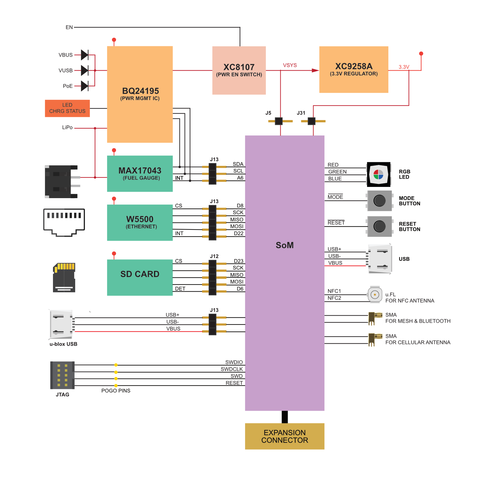
Block diagram
Description
Particle devices are certified for use only with specific cellular antennas that connect to the U.FL connector on the
module. Using an alternate antenna via the SMA connector (11) will require a lengthy and expensive recertification process.
Powering the board
The B-Series Eval Board can be powered by:
- There are two USB Micro B connectors on the eval board, be sure to use connector 3 "SOM USB".
- The B524/B523 require a LiPo battery when powering by USB due to the higher current requirements of 2G/3G. The B404X/B404/B402 (LTE Cat M1) can be powered by USB without a battery.
- When powering by VIN (barrel connector), 5-12 VDC is recommended, but up to 17 VDC can be supplied.
- Minimum power requirements are 5VDC @500mA (when using the LiPo battery) or 5VDC @2000mA (without LiPo battery).
- If purchasing a LiPo battery from a 3rd-party supplier, beware as the polarity of the JST-PH connector is not standardized and may be reversed. Permanent damage to the eval board can occur if powered by reverse polarity on the JST connector. See the battery guide for additional information.
- This board is not recommended for use with the M-SoM, however it can be used if you power it using the VIN barrel connector with a 12 watt power supply, 6V minimum.
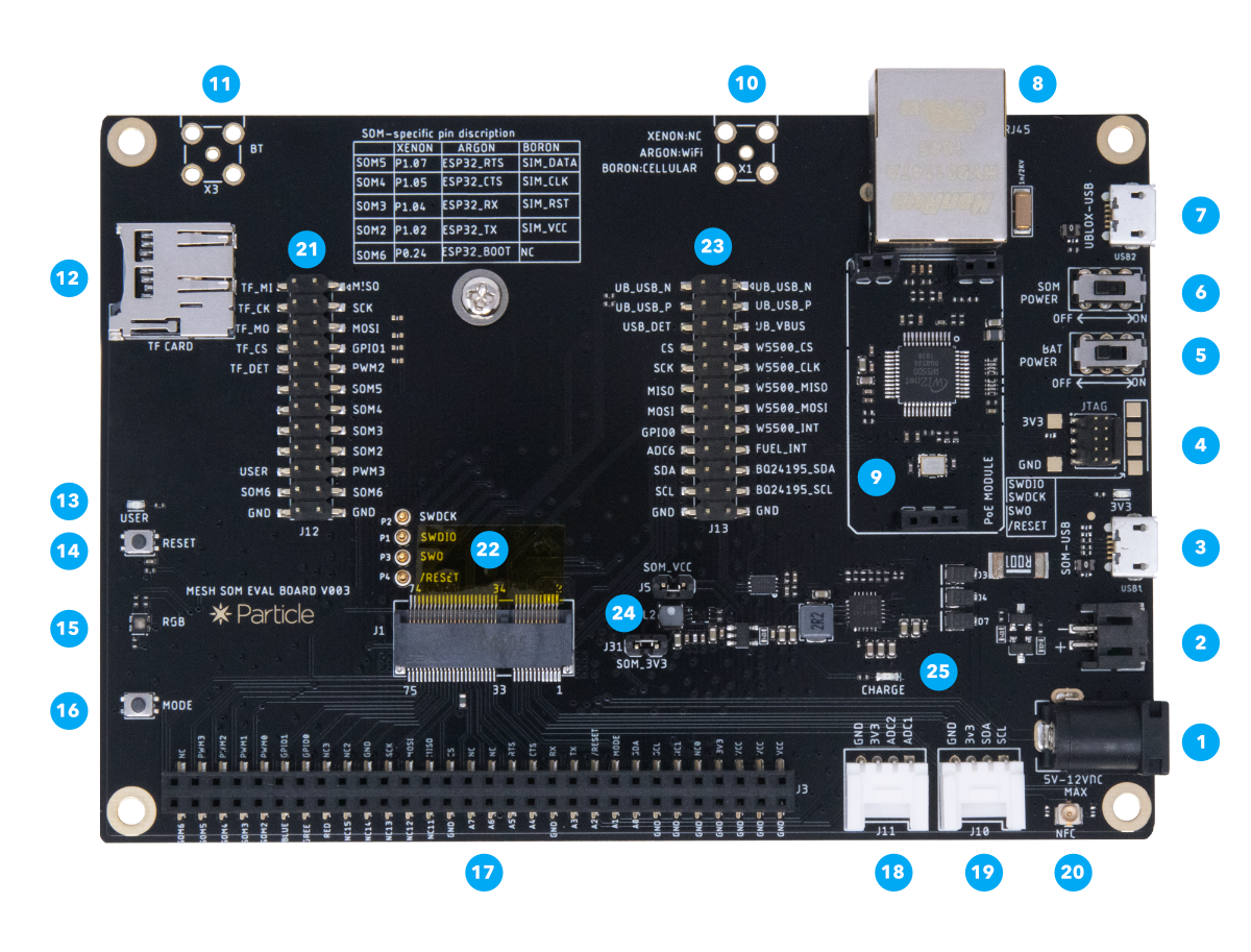
Jumpers J12
These pins are intended to be connected across using removable two-pin jumpers to connect features on the board to standard ports.
Jumpers J13
These pins are intended to be connected across using removable two-pin jumpers to connect features on the board to standard ports.
For more information about Ethernet, see the application note AN037 Ethernet.
Power jumpers
PWM Differences
On the B-Series SoM, pins D4, D5, D7, A0, A1, A6, and A7 can be used for PWM. Pins are assigned a PWM group. Each group must share the same
frequency and resolution, but individual pins in the group can have a different duty cycle.
- Group 2: Pins A0, A1, A6, and A7.
- Group 1: Pins D4, D5, and D6.
- Group 0: Pin D7 and the RGB LED. This must use the default resolution of 8 bits (0-255) and frequency of 500 Hz.
On Gen 3 Feather devices (Argon, Boron, Xenon), pins A0, A1, A2, A3, D2, D3, D4, D5, D6, D7, and D8 can be used for PWM. Pins are assigned a PWM group. Each group must share the same
frequency and resolution, but individual pins in the group can have a different duty cycle.
Group 3: Pins D2, D3, A4, and A5.
Group 2: Pins A0, A1, A2, and A3.
Group 1: Pins D4, D5, D6, and D8.
Group 0: Pin D7 and the RGB LED. This must use the default resolution of 8 bits (0-255) and frequency of 500 Hz.
These rules also apply to tone() (square wave with 50% duty cycle), however since each group must share the same frequency you can only generate two different simultaneous tones of different frequencies on the B-Series SoM. You cannot generate tone on group 0.
Basic setup
The basic setup for the B series to be operational is shown below:
- Plug the cellular antenna into the U.FL connector labeled CELL on the SoM. Remember never to power up this board without the antenna being connected. There is potential to damage the transmitter of the u-blox module if no antenna is connected.
- If you are going to use mobile app setup or BLE, connect the 2.4 GHz antenna (the smaller one) to the BT U.FL connector on the SoM.
- Connect power the USB (3) or a LiPo battery (4).
- Turn on the appropriate power switches (5).
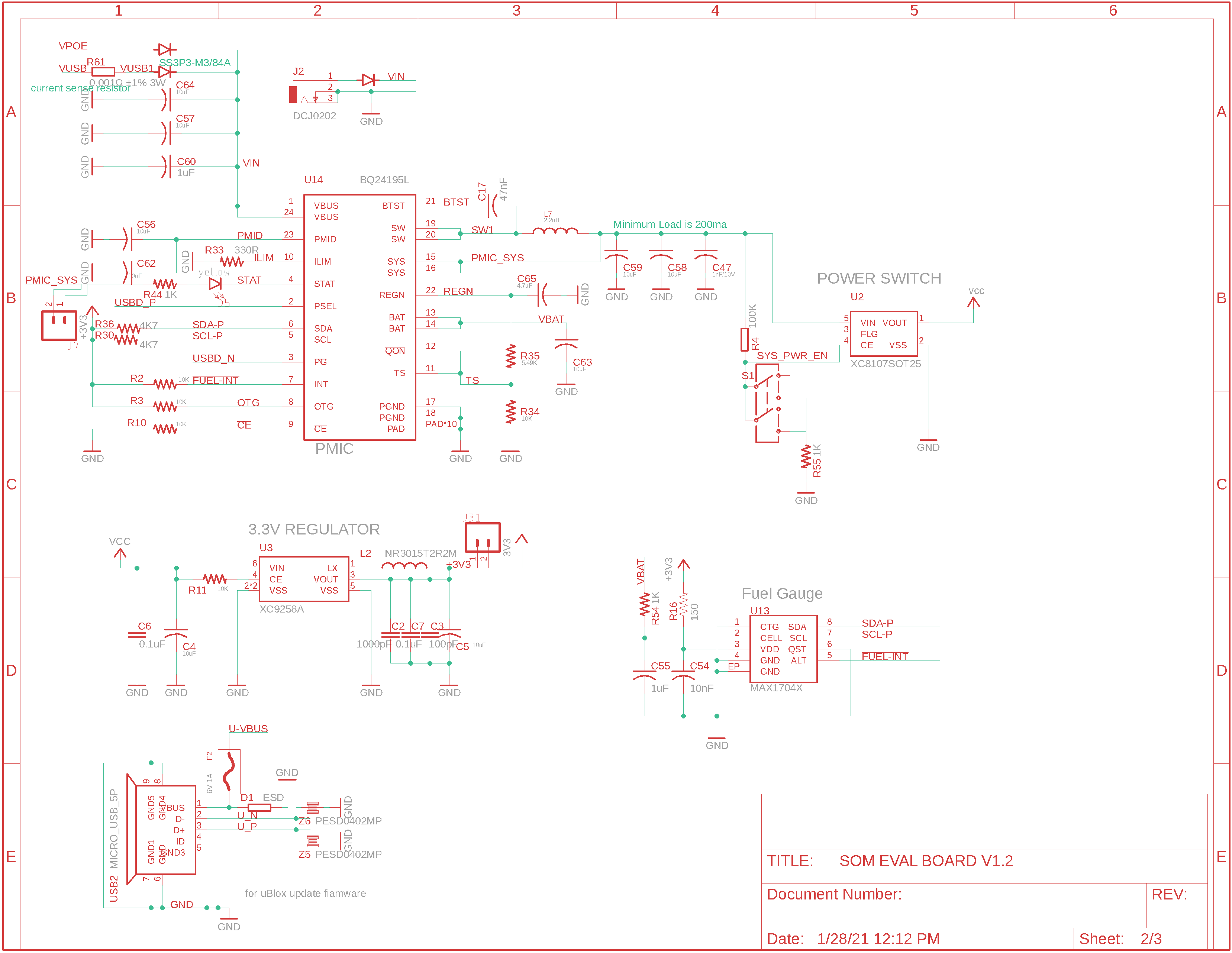
Using the PMIC and fuel gauge (recommended)
There is support for bq24195 PMIC and MAX17043 fuel gauge in Device OS so you don't need to add any additional configuration.
It requires these jumpers, which should be installed at the factory:
- ADC6 to PM_INT
- SDA to PM_SDA
- SCL to PM_SCL
If you are not using the PMIC be sure to remove the jumper if you need use pin A6 as an analog input or GPIO.
Power consumption
We do not recommend using the B-Series eval board for power consumption measurements. It's impossible to completely disconnect the Wiznet W5500 Ethernet interface without removing the chip from the board. This will result in significantly higher power consumption measurements than you would have in most applications.
Using the MicroSD card
To use the MicroSD card, you must add the jumpers for the SD_ pins.
You will normally use this with the SdFat library.
With the jumpers installed, it will use the secondary SPI (SPI1) and pin D5 as the chip select. You cannot use D2, D3, D4, D5, and D6 as GPIO for your own (non-SD card) use.
Note that SD_DET (D6 / PWM2) is an output. It's pulled high with a 47K resistor and driven low by a mechanical switch when a SD card is inserted. Be sure to remove the jumper if you are using D6 as regular GPIO.
Using ethernet
To use Ethernet, you must add the jumpers:
- CS to ETH_CS
- SCK to ETH_SCK
- MISO to ETH_MISO
- MOSI to ETH_MOSI
- GPIO0 to ETH_INT
With the jumpers installed, it will use the primary SPI and pins D8 as the chip select and D22 as the interrupt pin. You cannot use pins D8, D20, D22, or primary SPI (MISO, MOSI, SCK) as GPIO for your own (non-Ethernet) use. You can share SPI with other SPI peripherals that have libraries that correctly implement SPI transactions.
Using the Grove connectors
Labels
Note that some of the SOM labels on the M.2 eval board do not match the schematic net names. These are mostly NC pins
or a trivial difference, so the difference should not be noticeable.
- Pin: Pin number
- Name: Short name, often the name used in Device OS for MCU GPIO pins
- Label: The label on the M.2 eval board
- Net: The net name on the schematic
Full details
1 GND
| | Details |
| Pin Number | 1 |
| Pin Name | GND |
| Description | Ground. |
| M.2 connector pin number | 1 |
2 VCC
| | Details |
| Pin Number | 2 |
| Pin Name | VCC |
| Description | Cellular modem power. Typically 3.9V, can be 3.6V to 4.2V |
| M.2 connector pin number | 2 |
3 GND
| | Details |
| Pin Number | 3 |
| Pin Name | GND |
| Description | Ground. |
| M.2 connector pin number | 1 |
4 VCC
| | Details |
| Pin Number | 4 |
| Pin Name | VCC |
| Description | Cellular modem power. Typically 3.9V, can be 3.6V to 4.2V |
| M.2 connector pin number | 2 |
5 GND
| | Details |
| Pin Number | 5 |
| Pin Name | GND |
| Description | Ground. |
| M.2 connector pin number | 1 |
6 VCC
| | Details |
| Pin Number | 6 |
| Pin Name | VCC |
| Description | Cellular modem power. Typically 3.9V, can be 3.6V to 4.2V |
| M.2 connector pin number | 2 |
7 GND
| | Details |
| Pin Number | 7 |
| Pin Name | GND |
| Description | Ground. |
| M.2 connector pin number | 1 |
8 3V3
| | Details |
| Pin Number | 8 |
| Pin Name | 3V3 |
| Description | 3.3V used to power MCU |
| M.2 connector pin number | 10 |
9 GND
| | Details |
| Pin Number | 9 |
| Pin Name | GND |
| Description | Ground. |
| M.2 connector pin number | 1 |
10 SOM10
| | Details |
| Pin Number | 10 |
| Pin Name | SOM10 |
| Description | Not currently used, leave unconnected. |
| M.2 connector pin number | 14 |
11 SOM6
| | Details |
| Pin Number | 11 |
| Pin Name | SOM6 |
| Pin Alternate Name | NFC1 |
| Description | NFC Antenna 1. |
| MCU Pin | P0.09 |
| M.2 connector pin number | 17 |
12 SOM11
| | Details |
| Pin Number | 12 |
| Pin Name | SOM11 |
| Description | Not currently used, leave unconnected. |
| M.2 connector pin number | 18 |
13 SOM7
| | Details |
| Pin Number | 13 |
| Pin Name | SOM7 |
| Pin Alternate Name | NFC2 |
| Description | NFC Antenna 2. NFC2 is the center pin. |
| MCU Pin | P0.10 |
| M.2 connector pin number | 19 |
14 D1
| | Details |
| Pin Number | 14 |
| Pin Name | D1 |
| Pin Alternate Name | D1 |
| Description | I2C SCL. Cannot be used as GPIO. |
| Supports digitalRead | Yes |
| Supports digitalWrite | Yes |
| I2C interface | SCL. Use Wire object. |
| Supports attachInterrupt | Yes. You can only have 8 active interrupt pins. |
| Internal pull resistance | 13K |
| MCU Pin | P0.27 |
| M.2 connector pin number | 20 |
15 A0
| | Details |
| Pin Number | 15 |
| Pin Name | A0 |
| Pin Alternate Name | D19 |
| Description | A0 Analog in, GPIO, PWM |
| Supports digitalRead | Yes |
| Supports digitalWrite | Yes |
| Supports analogRead | Yes |
| Supports analogWrite (PWM) | Yes |
| Supports tone | A0, A1, A6, and A7 must have the same frequency. |
| Supports attachInterrupt | Yes. You can only have 8 active interrupt pins. |
| Internal pull resistance | 13K |
| MCU Pin | P0.03 |
| M.2 connector pin number | 23 |
16 D0
| | Details |
| Pin Number | 16 |
| Pin Name | D0 |
| Pin Alternate Name | D0 |
| Description | I2C SDA. Cannot be used as GPIO. |
| Supports digitalRead | Yes |
| Supports digitalWrite | Yes |
| I2C interface | SDA. Use Wire object. |
| Supports attachInterrupt | Yes. You can only have 8 active interrupt pins. |
| Internal pull resistance | 13K |
| MCU Pin | P0.26 |
| M.2 connector pin number | 22 |
17 A1
| | Details |
| Pin Number | 17 |
| Pin Name | A1 |
| Pin Alternate Name | D18 |
| Description | A1 Analog in, GPIO, PWM |
| Supports digitalRead | Yes |
| Supports digitalWrite | Yes |
| Supports analogRead | Yes |
| Supports analogWrite (PWM) | Yes |
| Supports tone | A0, A1, A6, and A7 must have the same frequency. |
| Supports attachInterrupt | Yes. You can only have 8 active interrupt pins. |
| Internal pull resistance | 13K |
| MCU Pin | P0.04 |
| M.2 connector pin number | 33 |
18 MODE
| | Details |
| Pin Number | 18 |
| Pin Name | MODE |
| Pin Alternate Name | D20 |
| Description | MODE button, has internal pull-up |
| MCU Pin | P0.11 |
| M.2 connector pin number | 32 |
19 A2
| | Details |
| Pin Number | 19 |
| Pin Name | A2 |
| Pin Alternate Name | D17 |
| Description | A2 Analog in, GPIO |
| Supports digitalRead | Yes |
| Supports digitalWrite | Yes |
| Supports analogRead | Yes |
| Supports attachInterrupt | Yes. You can only have 8 active interrupt pins. |
| Internal pull resistance | 13K |
| MCU Pin | P0.28 |
| M.2 connector pin number | 35 |
20 RST
| | Details |
| Pin Number | 20 |
| Pin Name | RST |
| Description | Hardware reset, active low. |
| M.2 connector pin number | 34 |
21 A3
| | Details |
| Pin Number | 21 |
| Pin Name | A3 |
| Pin Alternate Name | D16 |
| Description | A3 Analog in, GPIO |
| Supports digitalRead | Yes |
| Supports digitalWrite | Yes |
| Supports analogRead | Yes |
| Supports attachInterrupt | Yes. You can only have 8 active interrupt pins. |
| Internal pull resistance | 13K |
| MCU Pin | P0.29 |
| M.2 connector pin number | 37 |
22 TX
| | Details |
| Pin Number | 22 |
| Pin Name | TX |
| Pin Alternate Name | D9 |
| Description | Serial TX, GPIO |
| Supports digitalRead | Yes |
| Supports digitalWrite | Yes |
| UART serial | TX. Use Serial1 object. |
| Supports attachInterrupt | Yes. You can only have 8 active interrupt pins. |
| Internal pull resistance | 13K |
| MCU Pin | P0.06 |
| M.2 connector pin number | 36 |
23 GND
| | Details |
| Pin Number | 23 |
| Pin Name | GND |
| Description | Ground. |
| M.2 connector pin number | 1 |
24 RX
| | Details |
| Pin Number | 24 |
| Pin Name | RX |
| Pin Alternate Name | D10 |
| Description | Serial RX, GPIO |
| Supports digitalRead | Yes |
| Supports digitalWrite | Yes |
| UART serial | RX. Use Serial1 object. |
| Supports attachInterrupt | Yes. You can only have 8 active interrupt pins. |
| Internal pull resistance | 13K |
| MCU Pin | P0.08 |
| M.2 connector pin number | 38 |
25 A4
| | Details |
| Pin Number | 25 |
| Pin Name | A4 |
| Pin Alternate Name | D15 |
| Description | A4 Analog in, GPIO |
| Supports digitalRead | Yes |
| Supports digitalWrite | Yes |
| Supports analogRead | Yes |
| Supports attachInterrupt | Yes. You can only have 8 active interrupt pins. |
| Internal pull resistance | 13K |
| MCU Pin | P0.30 |
| M.2 connector pin number | 41 |
26 D3
| | Details |
| Pin Number | 26 |
| Pin Name | D3 |
| Pin Alternate Name | CTS |
| Description | SPI1 MOSI, Serial1 CTS, GPIO, Wire1 SCL |
| Supports digitalRead | Yes |
| Supports digitalWrite | Yes |
| UART serial | CTS. Use Serial1 object. |
| SPI interface | MOSI. Use SPI1 object. |
| I2C interface | SCL. Use Wire1 object. |
| Supports attachInterrupt | Yes. You can only have 8 active interrupt pins. |
| Internal pull resistance | 13K |
| MCU Pin | P1.01 |
| M.2 connector pin number | 40 |
27 A5
| | Details |
| Pin Number | 27 |
| Pin Name | A5 |
| Pin Alternate Name | D14 |
| Description | A5 Analog in, GPIO |
| Supports digitalRead | Yes |
| Supports digitalWrite | Yes |
| Supports analogRead | Yes |
| Supports attachInterrupt | Yes. You can only have 8 active interrupt pins. |
| Internal pull resistance | 13K |
| MCU Pin | P0.31 |
| M.2 connector pin number | 43 |
28 D2
| | Details |
| Pin Number | 28 |
| Pin Name | D2 |
| Pin Alternate Name | RTS |
| Description | SPI1 SCK, Serial1 RTS, PWM, GPIO, Wire1 SDA |
| Supports digitalRead | Yes |
| Supports digitalWrite | Yes |
| UART serial | RTS. Use Serial1 object. |
| SPI interface | SCK. Use SPI1 object. |
| I2C interface | SDA. Use Wire1 object. |
| Supports attachInterrupt | Yes. You can only have 8 active interrupt pins. |
| Internal pull resistance | 13K |
| MCU Pin | P1.02 |
| M.2 connector pin number | 42 |
29 A6
| | Details |
| Pin Number | 29 |
| Pin Name | A6 |
| Pin Alternate Name | D16 |
| Description | A6 Analog in, PWM, GPIO |
| Supports digitalRead | Yes |
| Supports digitalWrite | Yes |
| Supports analogRead | Yes |
| Supports analogWrite (PWM) | Yes |
| Supports tone | A0, A1, A6, and A7 must have the same frequency. |
| Supports attachInterrupt | Yes. You can only have 8 active interrupt pins. |
| Internal pull resistance | 13K |
| MCU Pin | P0.05 |
| M.2 connector pin number | 45 |
30 SOM0
| | Details |
| Pin Number | 30 |
| Pin Name | SOM0 |
| Pin Alternate Name | CELL USBD+ |
| Description | Cellular Modem USB Data+. |
| Input is 5V Tolerant | Yes |
| M.2 connector pin number | 44 |
31 A7
| | Details |
| Pin Number | 31 |
| Pin Name | A7 |
| Pin Alternate Name | D17 |
| Description | A7 Analog in, GPIO |
| Supports digitalRead | Yes |
| Supports digitalWrite | Yes |
| Supports analogRead | Yes |
| Supports analogWrite (PWM) | Yes |
| Supports tone | A0, A1, A6, and A7 must have the same frequency. |
| Supports attachInterrupt | Yes. You can only have 8 active interrupt pins. |
| Internal pull resistance | 13K |
| MCU Pin | P0.02 |
| M.2 connector pin number | 47 |
32 SOM1
| | Details |
| Pin Number | 32 |
| Pin Name | SOM1 |
| Pin Alternate Name | CELL USBD- |
| Description | Cellular Modem USB Data-. |
| Input is 5V Tolerant | Yes |
| M.2 connector pin number | 46 |
33 GND
| | Details |
| Pin Number | 33 |
| Pin Name | GND |
| Description | Ground. |
| M.2 connector pin number | 1 |
34 D8
| | Details |
| Pin Number | 34 |
| Pin Name | D8 |
| Pin Alternate Name | CS |
| Description | GPIO, SPI SS |
| Supports digitalRead | Yes |
| Supports digitalWrite | Yes |
| SPI interface | SS. Use SPI object. This is only the default SS/CS pin, you can use any GPIO instead. |
| Supports attachInterrupt | Yes. You can only have 8 active interrupt pins. |
| Internal pull resistance | 13K |
| MCU Pin | P1.03 |
| M.2 connector pin number | 48 |
35 SOM14
| | Details |
| Pin Number | 35 |
| Pin Name | SOM14 |
| Description | M.2 pin 51. Not currently used, leave unconnected. |
| M.2 connector pin number | 51 |
36 MISO
| | Details |
| Pin Number | 36 |
| Pin Name | MISO |
| Pin Alternate Name | D11 |
| Description | SPI MISO, GPIO |
| Supports digitalRead | Yes |
| Supports digitalWrite | Yes |
| SPI interface | MISO. Use SPI object. |
| Supports attachInterrupt | Yes. You can only have 8 active interrupt pins. |
| Internal pull resistance | 13K |
| MCU Pin | P1.14 |
| M.2 connector pin number | 50 |
37 SOM15
| | Details |
| Pin Number | 37 |
| Pin Name | SOM15 |
| Description | M.2 pin 53. Not currently used, leave unconnected. |
| M.2 connector pin number | 53 |
38 MOSI
| | Details |
| Pin Number | 38 |
| Pin Name | MOSI |
| Pin Alternate Name | D12 |
| Description | SPI MOSI, GPIO |
| Supports digitalRead | Yes |
| Supports digitalWrite | Yes |
| SPI interface | MOSI. Use SPI object. |
| Supports attachInterrupt | Yes. You can only have 8 active interrupt pins. |
| Internal pull resistance | 13K |
| MCU Pin | P1.13 |
| M.2 connector pin number | 52 |
39 SOM16
| | Details |
| Pin Number | 39 |
| Pin Name | SOM16 |
| Description | M.2 pin 55. Not currently used, leave unconnected. |
| M.2 connector pin number | 55 |
40 SCK
| | Details |
| Pin Number | 40 |
| Pin Name | SCK |
| Pin Alternate Name | D13 |
| Description | SPI SCK, GPIO |
| Supports digitalRead | Yes |
| Supports digitalWrite | Yes |
| SPI interface | SCK. Use SPI object. |
| Supports attachInterrupt | Yes. You can only have 8 active interrupt pins. |
| Internal pull resistance | 13K |
| MCU Pin | P1.15 |
| M.2 connector pin number | 54 |
41 SOM17
| | Details |
| Pin Number | 41 |
| Pin Name | SOM17 |
| Description | M.2 pin 57. Not currently used, leave unconnected. |
| M.2 connector pin number | 57 |
42 GND
| | Details |
| Pin Number | 42 |
| Pin Name | GND |
| Description | Ground. |
| M.2 connector pin number | 1 |
43 SOM18
| | Details |
| Pin Number | 43 |
| Pin Name | SOM18 |
| Description | M.2 pin 59. Not currently used, leave unconnected. |
| M.2 connector pin number | 59 |
44 SOM12
| | Details |
| Pin Number | 44 |
| Pin Name | SOM12 |
| Description | M.2 pin 58. Not currently used, leave unconnected. |
| M.2 connector pin number | 58 |
45 RGBR
| | Details |
| Pin Number | 45 |
| Pin Name | RGBR |
| Description | RGB LED Red |
| MCU Pin | P0.13 |
| M.2 connector pin number | 61 |
46 SOM13
| | Details |
| Pin Number | 46 |
| Pin Name | SOM13 |
| Description | M.2 pin 60. Not currently used, leave unconnected. |
| M.2 connector pin number | 60 |
47 RGBG
| | Details |
| Pin Number | 47 |
| Pin Name | RGBG |
| Description | RGB LED Green |
| MCU Pin | P0.14 |
| M.2 connector pin number | 63 |
48 D22
| | Details |
| Pin Number | 48 |
| Pin Name | D22 |
| Pin Alternate Name | GPIO0 |
| Description | GPIO D22 |
| Supports digitalRead | Yes |
| Supports digitalWrite | Yes |
| Supports attachInterrupt | Yes. You can only have 8 active interrupt pins. |
| Internal pull resistance | 13K |
| MCU Pin | P0.24 |
| M.2 connector pin number | 62 |
49 RGBB
| | Details |
| Pin Number | 49 |
| Pin Name | RGBB |
| Description | RGB LED Blue |
| MCU Pin | P0.15 |
| M.2 connector pin number | 65 |
50 D23
| | Details |
| Pin Number | 50 |
| Pin Name | D23 |
| Pin Alternate Name | GPIO1 |
| Description | GPIO D23 |
| Supports digitalRead | Yes |
| Supports digitalWrite | Yes |
| Supports attachInterrupt | Yes. You can only have 8 active interrupt pins. |
| Internal pull resistance | 13K |
| MCU Pin | P1.09 |
| M.2 connector pin number | 64 |
51 SOM5
| | Details |
| Pin Number | 51 |
| Pin Name | SOM5 |
| Pin Alternate Name | SIM_VCC |
| Description | Leave unconnected. External SIM support is not available on B-SoM. |
| M.2 connector pin number | 67 |
52 D4
| | Details |
| Pin Number | 52 |
| Pin Name | D4 |
| Pin Alternate Name | PWM0 |
| Description | SPI1 MISO, PWM, GPIO D4 |
| Supports digitalRead | Yes |
| Supports digitalWrite | Yes |
| Supports analogWrite (PWM) | Yes |
| Supports tone | D4, D5, and D6 must have the same frequency. |
| SPI interface | MISO. Use SPI1 object. |
| Supports attachInterrupt | Yes. You can only have 8 active interrupt pins. |
| Internal pull resistance | 13K |
| MCU Pin | P1.08 |
| M.2 connector pin number | 66 |
53 SOM6
| | Details |
| Pin Number | 53 |
| Pin Name | SOM6 |
| Pin Alternate Name | SIM_RST |
| Description | Leave unconnected. External SIM support is not available on B-SoM. |
| M.2 connector pin number | 69 |
54 D5
| | Details |
| Pin Number | 54 |
| Pin Name | D5 |
| Pin Alternate Name | PWM1 |
| Description | PWM, GPIO D5 |
| Supports digitalRead | Yes |
| Supports digitalWrite | Yes |
| Supports analogWrite (PWM) | Yes |
| Supports tone | D4, D5, and D6 must have the same frequency. |
| Supports attachInterrupt | Yes. You can only have 8 active interrupt pins. |
| Internal pull resistance | 13K |
| MCU Pin | P1.10 |
| M.2 connector pin number | 68 |
55 SOM7
| | Details |
| Pin Number | 55 |
| Pin Name | SOM7 |
| Pin Alternate Name | SIM_CLK |
| Description | Leave unconnected, 1.8V/3V SIM Clock Output from R410M. |
| M.2 connector pin number | 71 |
56 D6
| | Details |
| Pin Number | 56 |
| Pin Name | D6 |
| Pin Alternate Name | PWM2 |
| Description | PWM, GPIO D6 |
| Supports digitalRead | Yes |
| Supports digitalWrite | Yes |
| Supports analogWrite (PWM) | Yes |
| Supports tone | D4, D5, and D6 must have the same frequency. |
| Supports attachInterrupt | Yes. You can only have 8 active interrupt pins. |
| Internal pull resistance | 13K |
| MCU Pin | P1.11 |
| M.2 connector pin number | 70 |
57 SOM8
| | Details |
| Pin Number | 57 |
| Pin Name | SOM8 |
| Pin Alternate Name | SIM_DATA |
| Description | Leave unconnected. External SIM support is not available on B-SoM. |
| M.2 connector pin number | 73 |
58 D7
| | Details |
| Pin Number | 58 |
| Pin Name | D7 |
| Pin Alternate Name | PWM3 |
| Description | PWM, GPIO D7, Blue LED |
| Supports digitalRead | Yes |
| Supports digitalWrite | Yes |
| Supports analogWrite (PWM) | PWM is shared with the RGB LED, you can specify a different duty cycle but should not change the frequency. |
| Supports attachInterrupt | Yes. You can only have 8 active interrupt pins. |
| Internal pull resistance | 13K |
| MCU Pin | P1.12 |
| M.2 connector pin number | 72 |
59 GND
| | Details |
| Pin Number | 59 |
| Pin Name | GND |
| Description | Ground. |
| M.2 connector pin number | 1 |
60 SOM9
| | Details |
| Pin Number | 60 |
| Pin Name | SOM9 |
| Description | M.2 pin 75. Not currently used, leave unconnected. |
| M.2 connector pin number | 75 |
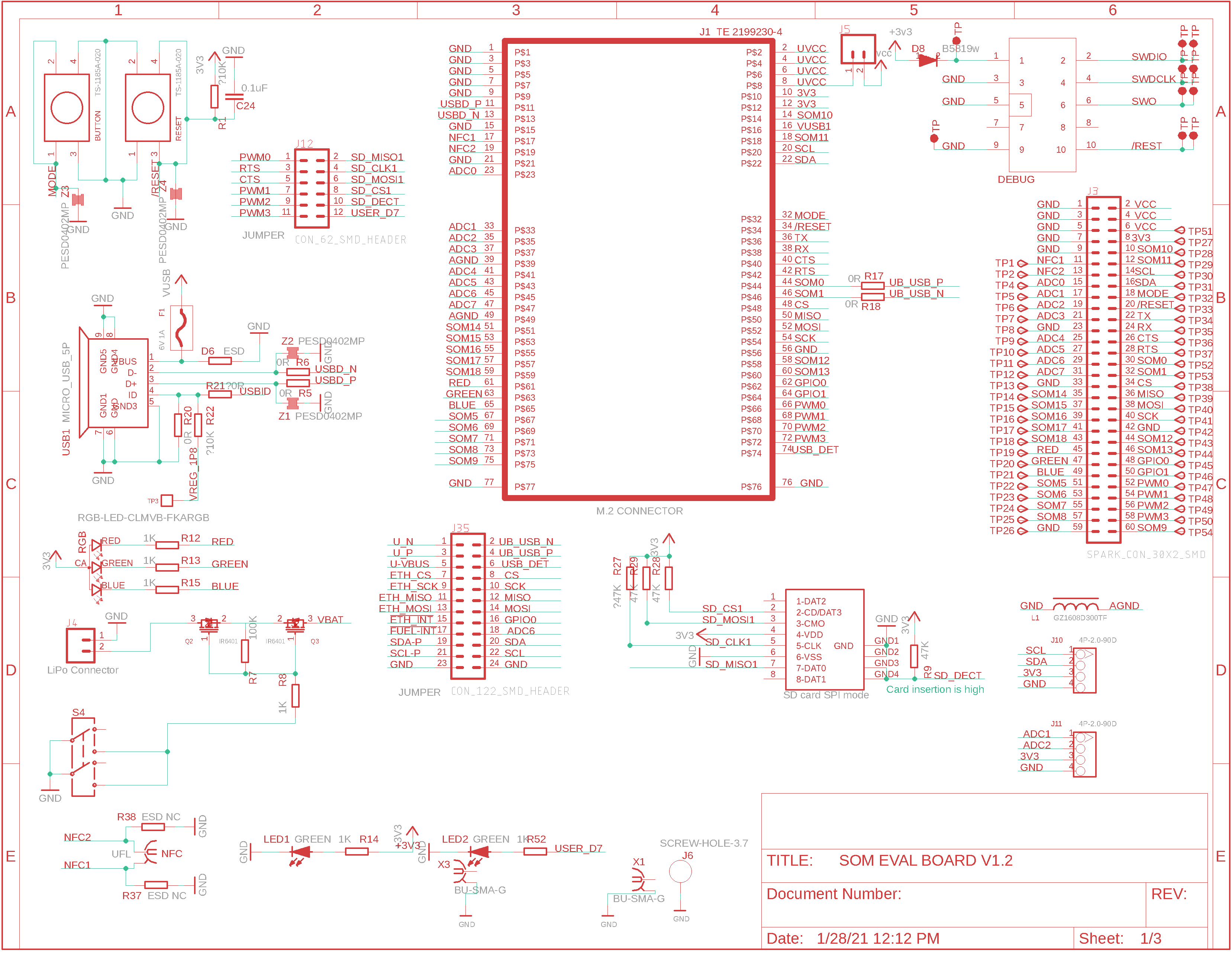
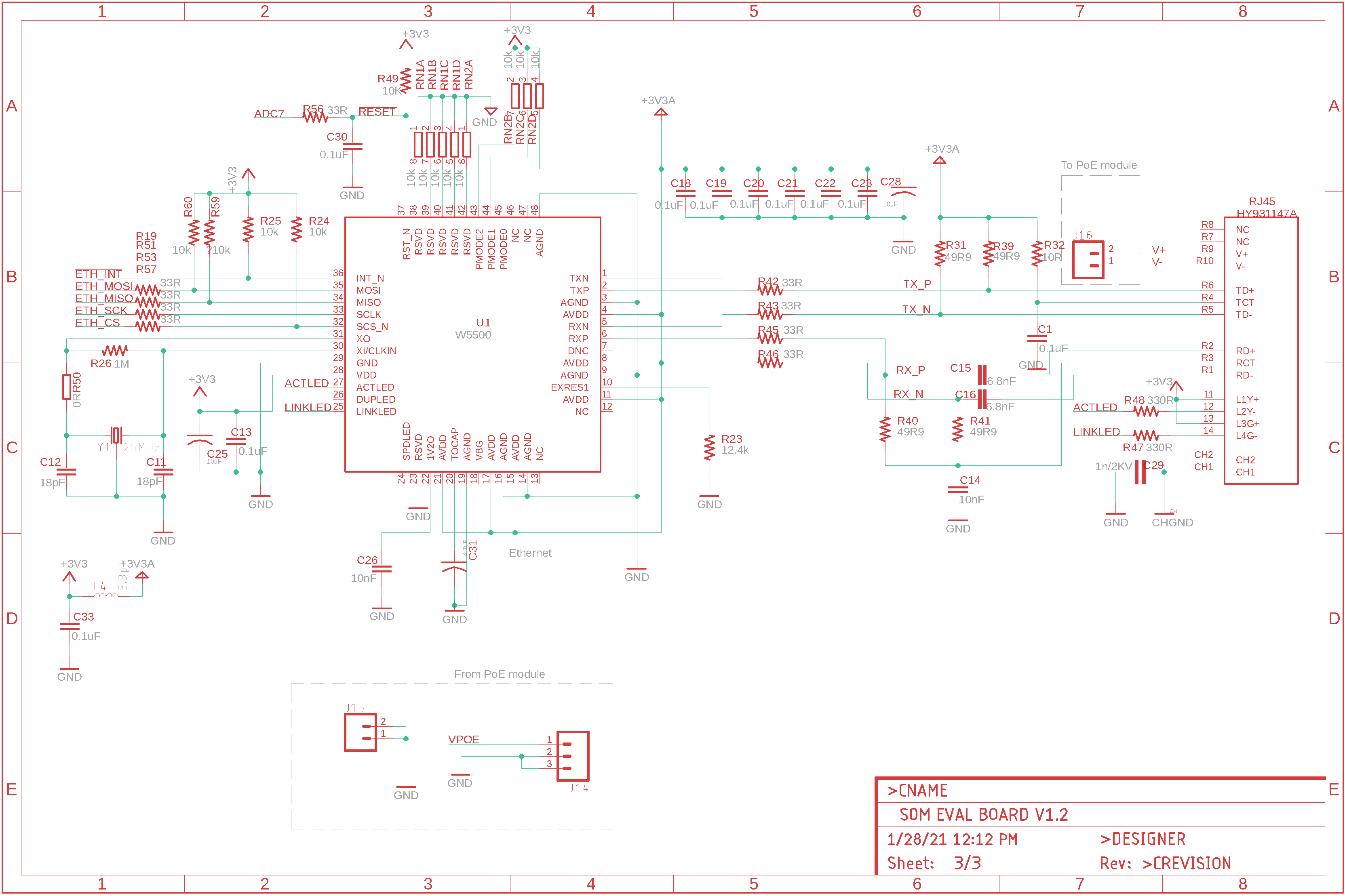
Evaluation board schematics
Page 1
Page 2
Page 3
Mechanical specifications
Dimensions and weight
Revision history