
E404X Datasheet
Functional description
Overview
The E404X is a LTE Cat M1 cellular device with support for BLE (Bluetooth LE). It is based on the Nordic nRF52840 microcontroller shared with other Gen 3 devices such as the Boron and B-Series SoM. It is only intended for use in the United States, Canada, and Mexico.
It is a SMD module designed to be reflowed to your own custom base board and is the same size and has a nearly identical pin-out to the E-Series module.
If you are migrating from the E402 or E404, there is a migration guide available.
There will not be 2G/3G "X" version E-Series; there will not be an E310X or E314X.
New designs should use the B404X (B-Series SoM) instead of the E404X.
Features
- u-blox SARA-R510S-01B LTE modem
- LTE Cat M1 module
- Support for United States, Canada, and Mexico only
- 3GPP Release 14 LTE Cat M1
- Cat M1 bands: 2, 4, 5, 12, 13
- Embedded Particle EtherSIM
- Nordic Semiconductor nRF52840 SoC
- ARM Cortex-M4F 32-bit processor @ 64MHz
- 1MB flash, 256KB RAM
- Bluetooth 5: 2 Mbps, 1 Mbps, 500 Kbps, 125 Kbps
- Supports DSP instructions, HW accelerated Floating Point Unit (FPU) and encryption functions
- Up to +8 dBm TX power (down to -20 dBm in 4 dB steps)
- On-module additional 4MB SPI flash
- 24 mixed signal GPIO (8 x Analog, 4 x PWM), UART, I2C, SPI
- USB 2.0 full speed (12 Mbps)
- Included PMIC and Fuel Gauge for easy use in battery-powered applications
- JTAG (SWD) pins
- Pins for RGB LED used for connection status
- Pins for reset and mode buttons
- On-module MFF2 Particle SIM
- Two on-module U.FL connectors for external antennas
- FCC (United States) and ISED (Canada) certified
- RoHS compliant (lead-free)
- Requires Device OS 4.0.0 LTS (or later)
Device OS support
It is recommended that you use the latest version in the 4.x LTS release line with the E404X. The minimum required version is 4.0.0. You cannot use the E404X with Device OS 2.x LTS.
For information on upgrading Device OS, see Version information. For the latest version shipped from the factory, see Manufacturing firmware versions page. See also Long Term Support (LTS) releases.
Interfaces
Block diagram
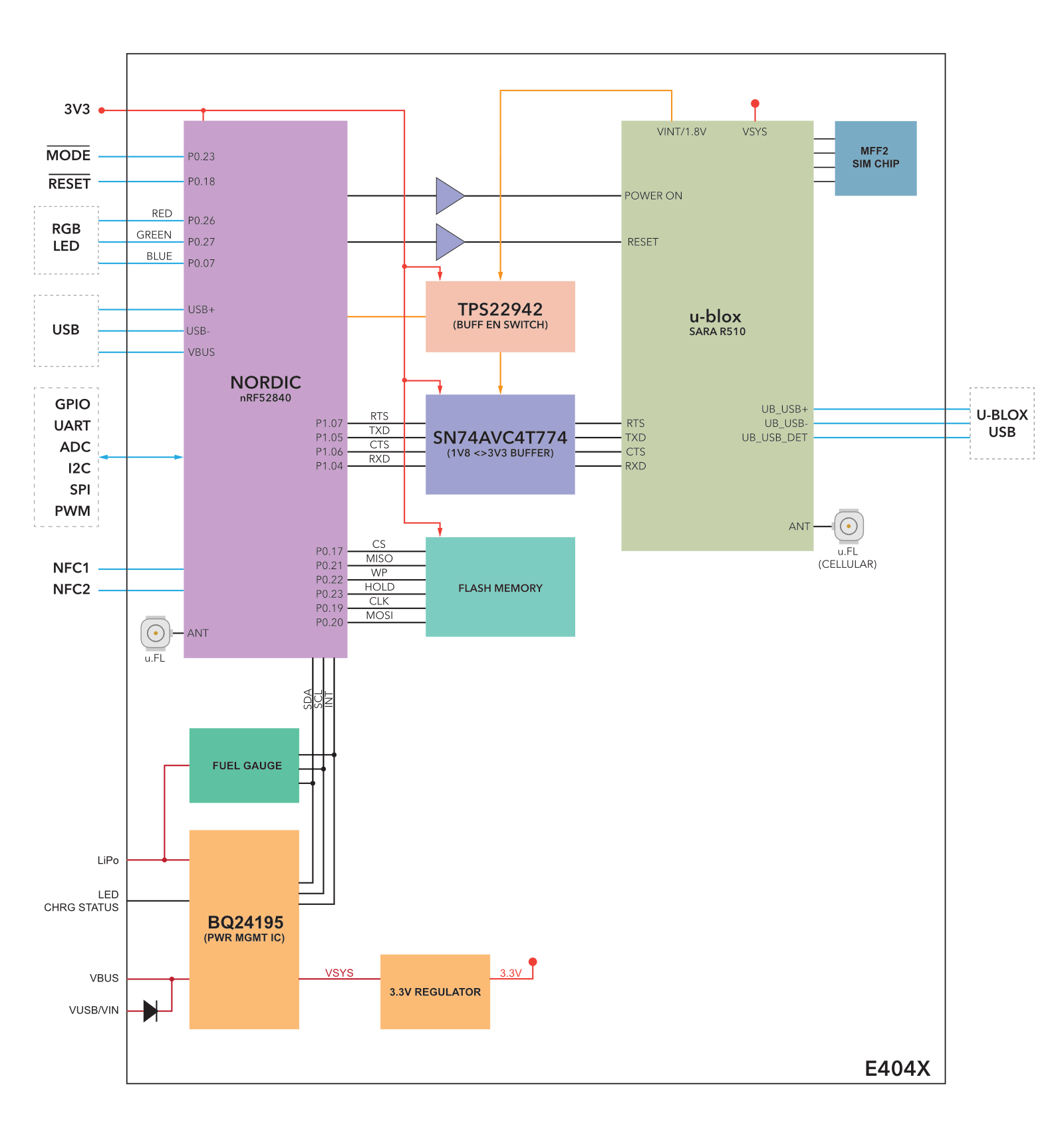
This diagram for illustration only and is subject to change
Power
The E series can be powered via the VIN (3.88V-12VDC) pin, over USB, or a LiPo battery.
VIN
The input voltage range on VIN pin is 3.88VDC to 12VDC. When powering from the VIN pin alone, make sure that the power supply is rated at 10W (for example 5 VDC at 2 Amp). If the power source is unable to meet this requirement, you'll need connect the LiPo battery as well. An additional bulk capacitance of 470uF to 1000uF should be added to the VIN input when the LiPo Battery is disconnected. The amount of capacitance required will depend on the ability of the power supply to deliver peak currents to the cellular modem.
The E404X can be powered with as little as 550 mA at 5V.
LiPo
This pin serves two purposes. You can use this pin to connect a LiPo battery directly without having to use a JST connector or it can be used to connect an external DC power source (and this is where one needs to take extra precautions). When powering it from an external regulated DC source, the recommended input voltage range on this pin is between 3.6V to 4.4VDC. Make sure that the supply can handle currents of at least 3Amp. This is the most efficient way of powering the E series since the PMIC by-passes the regulator and supplies power to the E series module via an internal FET leading to lower quiescent current.
When powered from a LiPo battery alone, the power management IC switches off the internal regulator and supplies power to the system directly from the battery. This reduces the conduction losses and maximizes battery run time. The battery provided with the E series module is a Lithium-Ion Polymer battery rated at 3.7VDC 1,800mAh. You can substitute this battery with another 3.7V LiPo with higher current rating. Remember to never exceed this voltage rating and always pay attention to the polarity of the connector.
Typical current consumption is around 180mA and up to 1.8A transients at 5VDC. In deep sleep mode, the quiescent current is 130uA (powered from the battery alone).
VBUS
This pin is internally connected to USB supply rail and will output 5V when the E series module is plugged into an USB port. It is intentionally left unpopulated. This pin will NOT output any voltage when the E series module is powered via VIN and/or the LiPo battery.
Most USB ports can supply only a maximum of 500mA, but the u-Blox GSM module on the E series alone can consume a peak of 800mA to 1800mA (2G/3G) or 550 mA (LTE Cat M1) of current during transmission. In order to compensate of this deficit, one must connect the LiPo battery at all times when powering from a traditional USB port for 2G/3G. The E series will intelligently source power from the USB most of the time and keep the battery charged. During peak current requirements, the additional power will be sourced from the battery. This reduces the charge-discharge cycle load on the battery, thus improving its longevity.
3V3 Pin
This pin is the output of the on-board 3.3V switching regulator that powers the microcontroller and the peripherals. This pin can be used as a 3.3V power source with a max load of 800mA. Unlike the Photon or the Core, this pin CANNOT be used as an input to power the E series module.
VBAT
This is the supply to the internal RTC, backup registers and SRAM. You can connect a backup battery to it (1.65 to 3.6VDC), if you wish to retain RTC/RAM when 3V3 is absent or simply tie it up to 3V3.
PMID
This pin is connected to the PMID pin of the bq24195 PMIC. You should leave this pin unconnected.
FCC approved antennas
| Antenna | SKU | Links |
|---|---|---|
| Wide band LTE-CAT M1 cell antenna, [x1] | PARANTC41EA | Datasheet |
| Wide band LTE-CAT M1 cell antenna, [x50] | PARANTC41TY | Datasheet |
| Taoglas Cellular Flex Antenna 2G/3G/LTE 5dBi, [x1] | ANT-FLXU | Datasheet | Retail Store |
| Taoglas Cellular Flex Antenna 2G/3G/LTE 5dBi, [x50] | ANT-FLXU-50 | Datasheet |
Bluetooth LE (BLE)
The E404X does not have a BLE chip antenna on the module and requires an external antenna if BLE is to be used. Using BLE on the E404X is optional, and the antenna is not required if BLE is not used.
The Particle 2.4 GHz BLE antenna is available in the retail and wholesale stores. Note: The same external antenna model is used for Wi-Fi and BLE.
| Antenna | SKU | Links |
|---|---|---|
| Particle Wi-Fi Antenna 2.4GHz, [x1] | ANT-FLXV2 | Datasheet | Retail Store |
| Particle Wi-Fi Antenna 2.4GHz, [x50] | ANT-FLXV2-50 | Datasheet |
General antenna guidance
- The antenna placement needs to follow some basic rules, as any antenna is sensitive to its environment. Mount the antenna at least 10mm from metal components or surfaces, ideally 20mm for best radiation efficiency, and try to maintain a minimum of three directions free from obstructions to be able to operate effectively.
- Needs tuning with actual product enclosure and all components.
- For the BLE antenna, it is recommended to use a 2.4 GHz single-frequency antenna and not a 2.4 GHz + 5 GHz antenna, so as to avoid large gain at the frequency twice of 2.4 GHz which can cause the second harmonic radiation of 2.4 GHz to exceed standards.
Peripherals and GPIO
| Peripheral Type | Qty | Input(I) / Output(O) |
|---|---|---|
| Digital | 22 (max) | I/O |
| Analog (ADC) | 8 (max) | I |
| UART | 1 | I/O |
| SPI | 2 | I/O |
| I2C | 1 | I/O |
| USB | 1 | I/O |
| PWM | 13 (max) | O |
GPIO
- GPIO is limited to 3.3V maximum (not 5V tolerant)
- If an alternate port such as SPI or Serial is not being used for that purpose, the pins can generally be used as GPIO
| Pin | E404X Pin Name | E404X GPIO |
|---|---|---|
| 16 | TX | ✓ |
| 17 | RX | ✓ |
| 19 | A7 / WKP | ✓ |
| 20 | A6 | ✓ |
| 21 | A5 | ✓ |
| 22 | A4 | ✓ |
| 23 | A3 | ✓ |
| 24 | A2 | ✓ |
| 25 | A1 | ✓ |
| 26 | A0 | ✓ |
| 30 | B3 | ✓ |
| 31 | B2 | ✓ |
| 32 | B1 | ✓ |
| 33 | B0 | ✓ |
| 37 | D5 | ✓ |
| 40 | D2 | ✓ |
| 41 | D1 | ✓ |
| 42 | D0 | ✓ |
| 44 | C5 | ✓ |
| 45 | C4 | ✓ |
| 46 | C3 | ✓ |
| 47 | C2 | ✓ |
| 48 | C1 | ✓ |
| 49 | C0 | ✓ |
ADC
The E404X supports 8 ADC inputs.
| Pin | E404X Pin Name | E404X ADC |
|---|---|---|
| 19 | A7 / WKP | ADC7 |
| 20 | A6 | ADC6 |
| 21 | A5 | ADC5 |
| 22 | A4 | ADC4 |
| 23 | A3 | ADC3 |
| 24 | A2 | ADC2 |
| 25 | A1 | ADC1 |
| 26 | A0 | ADC0 |
- ADC inputs are single-ended and limited to 0 to 3.3V
- Resolution is 12 bits
On the B404X, BRN404X, and E404X, the ADC reference is the nRF52840 internal 0.6V reference, with a 1/6 gain from the input pin. This is different than other Gen 3 devices which use 3V3 as the ADC reference.
This reference and gain combination is a range of 0 to 3.6V for 0 - 4095. This is scaled in software so 3.3V will still be 4095, so there will be a slight loss of resolution.
UART
- One available hardware UART (
Serial1). - Supported baud rates: 1200, 2400, 4800, 9600, 19200, 28800, 38400, 57600, 76800, 115200, 230400, 250000, 460800, 921600 and 1000000.
Configuration options include:
SERIAL_8N1- 8 data bits, no parity, 1 stop bit (default)SERIAL_8E1- 8 data bits, even parity, 1 stop bit
Other options, including odd parity, and 7 and 9 bit modes, are not available on the E404x or Gen 3 devices.
Flow control is available on Serial1 D3(CTS) and D2(RTS). If you are not using flow control (the default), then these pins can be used as regular GPIO.
SERIAL_FLOW_CONTROL_NONE- no flow controlSERIAL_FLOW_CONTROL_RTS- RTS flow controlSERIAL_FLOW_CONTROL_CTS- CTS flow controlSERIAL_FLOW_CONTROL_RTS_CTS- RTS/CTS flow control
| Pin | E404X Pin Name | E404X UART |
|---|---|---|
| 16 | TX | Serial1 (TX) |
| 17 | RX | Serial1 (RX) |
| 41 | D1 | Serial1 (CTS) |
| 42 | D0 | Serial1 (RTS) |
SPI
- Any available GPIO can be used for SPI chip select (SS).
- Generally speaking, multiple SPI devices can share a SPI bus, however the software library must enable it using SPI transactions
SPI_MODE_SLAVEis only supported onSPI1and is limited to 8 MHz.
| Pin | E404X Pin Name | E404X SPI |
|---|---|---|
| 21 | A5 | SPI (MOSI) |
| 22 | A4 | SPI (MISO) |
| 23 | A3 | SPI (SCK) |
| 24 | A2 | SPI (SS) |
| 37 | D5 | SPI1 (SS) |
| 46 | C3 | SPI1 (SCK) |
| 47 | C2 | SPI1 (MISO) |
| 48 | C1 | SPI1 (MOSI) |
I2C
There is one available I2C interface on the E404X.
| Pin | E404X Pin Name | E404X I2C |
|---|---|---|
| 41 | D1 | Wire (SCL) |
| 42 | D0 | Wire (SDA) |
PWM
| Pin | E404X Pin Name | E404X PWM |
|---|---|---|
| 16 | TX | ✓ |
| 17 | RX | ✓ |
| 20 | A6 | ✓ |
| 21 | A5 | ✓ |
| 22 | A4 | ✓ |
| 23 | A3 | ✓ |
| 30 | B3 | ✓ |
| 31 | B2 | ✓ |
| 40 | D2 | ✓ |
| 41 | D1 | ✓ |
| 42 | D0 | ✓ |
| 44 | C5 | ✓ |
| 45 | C4 | ✓ |
| 49 | C0 | ✓ |
On the E404X, the following groups are defined. Each group must share the same frequency and resolution, but individual pins in the group can have a different duty cycle. Group 0 is shared with the RGB LED and must use the default resolution of 8 bits (0-255) and frequency of 500 Hz, but can have its own duty cycle.
- Group 0: C5, RGBB, RGBG, RGBR
- Group 1: A3, C0, D0, D1, D2
- Group 2: B2, B3, RX, TX
- Group 3: A4, A5, A6, C4
JTAG AND SWD
The E404X has a SWD only on dedicated pins that cannot be used for GPIO.
| Module Pin | E-Series Pin | SWD |
|---|---|---|
| 35 | D7 | SWDIO |
| 36 | D6 | SWCLK |
| 38 | D4 | SWO |
| 56 | RESET | RESET |
The nRF52840 MCU on the E404X can be programmed by:
- Particle Debugger
- Other CMSIS-DAP Debugger (DAPLink)
- Segger J/LINK
It cannot be programmed by the ST-LINK/V2.
Complete module and pin listing

| Pin | Pin Name | Description | MCU |
|---|---|---|---|
| 1 | VIN | Power in 3.9V to 12 VDC. | |
| 2 | GND | Ground. Be sure to connect all GND pins. | |
| 3 | VBUS | Connect to VBUS power pin on the USB port | |
| 4 | GND | Ground. Be sure to connect all GND pins. | |
| 5 | LIPO | Connect to + pin on the LiPo battery, 4.2V maximum | |
| 6 | NC | Do not connect to anything | |
| 7 | GND | Ground. Be sure to connect all GND pins. | |
| 8 | PMID | Connected to the PMID pin of the PMIC. Leave unconnected. | |
| 9 | 3V3 | Regulated 3.3V DC output, maximum load 800 mA. Cannot be used as a power input. | |
| 10 | NC | Do not connect to anything | |
| 11 | NC | Do not connect to anything | |
| 12 | GND | Ground. Be sure to connect all GND pins. | |
| 13 | USBDATA+ | USB Data+. Cannot be used as GPIO. | D+ |
| 14 | USBDATA- | USB Data-. Cannot be used as GPIO. | D- |
| 15 | GND | Ground. Be sure to connect all GND pins. | |
| 16 | TX | Serial1 TX (transmitted data), GPIO D8, PWM. | P0.06 |
| 17 | RX | Serial1 RX (received data), GPIO D9, PWM. | P0.08 |
| 18 | GND | Ground. Be sure to connect all GND pins. | |
| 19 | A7 / WKP | A7 analog in, WKP (wakeup), GPIO D17. | P0.05 |
| 20 | A6 | A6 analog in, PWM, GPIO D16. | P0.04 |
| 21 | A5 | A5 Analog in, GPIO D15, SPI MOSI, PWM. | P0.31 |
| 22 | A4 | A4 Analog in, GPIO D14, SPI MISO, PWM. | P0.30 |
| 23 | A3 | A3 analog in, GPIO D13, SPI SCK, PWM | P0.29 |
| 24 | A2 | A2 Analog in, GPIO D12, SPI SS | P0.28 |
| 25 | A1 | A1 Analog in, GPIO D11 | P0.02 |
| 26 | A0 | A0 Analog in, GPIO D10 | P0.03 |
| 27 | GND | Ground. Be sure to connect all GND pins. | |
| 28 | NC | Do not connect to anything | |
| 29 | NC | Do not connect to anything | |
| 30 | B3 | B3, GPIO D21, PWM | P1.13 |
| 31 | B2 | B2, GPIO D20, PWM | P1.12 |
| 32 | B1 | B1, GPIO D19 | P0.09 |
| 33 | B0 | B0, GPIO D18 | P0.10 |
| 34 | GND | Ground. Be sure to connect all GND pins. | |
| 35 | SWDIO | SWDIO for JTAG/SWD debugger. Internal pull-up. Not GPIO. | SWDIO |
| 36 | SWDCLK | SWCLK for JTAG/SWD debugger. Internal pull-down. Not GPIO. | SWCLK |
| 37 | D5 | D5 GPIO, SPI1 SS | P1.11 |
| 38 | SWO | SWO for JTAG/SWD debugger. Not GPIO. | SWO |
| 39 | NC | Do not connect to anything | |
| 40 | D2 | D2 GPIO, PWM | P1.10 |
| 41 | D1 | D0 GPIO, I2C Wire SCL, Serial1 RTS, PWM | P1.02 |
| 42 | D0 | D0 GPIO, I2C Wire SDA, Serial1 CTS, PWM | 1.01 |
| 43 | GND | Ground. Be sure to connect all GND pins. | |
| 44 | C5 | GPIO D29, PWM | P1.03 |
| 45 | C4 | GPIO D28, PWM | P0.24 |
| 46 | C3 | SPI1 SCK, GPIO D27. | P0.12 |
| 47 | C2 | SPI1 MISO, GPIO D26. | P0.11 |
| 48 | C1 | SPI1 MOSI, GPIO D25. | P1.09 |
| 49 | C0 | GPIO D24, PWM. | P1.08 |
| 50 | NC | Do not connect to anything | |
| 51 | GND | Ground. Be sure to connect all GND pins. | |
| 52 | RGBB | RGB LED Blue | P0.07 |
| 53 | RGBG | RGB LED Green | P0.27 |
| 54 | RGBR | RGB LED Red | P0.26 |
| 55 | MODE | MODE button, has internal pull-up. Pin number constant is BTN. | P0.25 |
| 56 | RESET | Hardware reset. Pull low to reset; can leave unconnected in normal operation. | P0.18 |
| 57 | STAT | Charge status output from the PMIC. | |
| 58 | GND | Ground. Be sure to connect all GND pins. | |
| 59 | GND | Ground. Be sure to connect all GND pins. | |
| 60 | GND | Ground. Be sure to connect all GND pins. |
Memory map
nRF52840 flash layout overview
- Bootloader (48KB, @0xF4000)
- User Application
- 256KB @ 0xB4000 (Device OS 3.1 and later)
- 128KB @ 0xD4000 (Device OS 3.0 and earlier)
- System (656KB, @0x30000)
- SoftDevice (192KB)
External SPI flash layout overview (dfu offset: 0x80000000)
- OTA (1500KB, @0x00289000)
- Reserved (420KB, @0x00220000)
- FAC (128KB, @0x00200000)
- LittleFS (2M, @0x00000000)
Pin and button definition
Pin markings:
To be provided later
LED Status
Charge status LED
| State | Description |
|---|---|
| ON | Charging in progress |
| OFF | Charging complete |
| Blink at 1Hz | Fault condition[1] |
| Rapid blinking | Battery disconnected[2] |
Notes:
[1] A fault condition can occur due to several reasons, for example, battery over/under voltage, temperature fault or safety timer fault. You can find the root cause by reading the fault register of the power management IC in firmware.
[2] You can stop this behavior by either plugging in the LiPo battery or by disabling the charging using the appropriate firmware command.
System RGB LED
Unlike the Electron, the E series module does not have an on-board RGB status LED. We have provided its individual control pins for you to connect an LED of your liking. This will allow greater flexibility in the end design of your products.
For a detailed explanation of different color codes of the RGB system LED, please take a look here.
LED status
System RGB LED
Unlike the Boron or Electron, the E404X module does not have an on-module RGB system status LED. We have provided its individual control pins for you to connect an LED of your liking. This will allow greater flexibility in the end design of your products.
A detailed explanation of different color codes of the RGB system LED can be found here.
Technical specifications
Absolute maximum ratings [1]
Supply voltages
| Parameter | Symbol | Min | Typ | Max | Unit |
|---|---|---|---|---|---|
| Supply voltages | |||||
| Supply Input Voltage | VCC | -0.3 | +6.0 | V | |
| Supply Input Voltage | 3V3 | -0.3 | +3.9 | V | |
| VBUS USB supply voltage | VUSB | -0.3 | +5.8 | V | |
| I/O pin voltage | |||||
| VI/O, VDD ≤ 3.6 V | IO | -0.3 | VDD + 0.3 | V | |
| VI/O, VDD > 3.6 V | IO | -0.3 | +3.9 | V | |
| Radio | |||||
| BT RF input level (52840) | 10 | dBm | |||
| Environmental | |||||
| Storage temperature | -40 | +85 | °C |
[1] Stresses beyond those listed under absolute maximum ratings may cause permanent damage to the device. These are stress ratings only, and functional operation of the device at these or any other conditions beyond those indicated under recommended operating conditions is not implied. Exposure to absolute-maximum-rated conditions for extended periods may affect device reliability.
Recommended operating conditions
| Parameter | Symbol | Min | Typ | Max | Unit |
|---|---|---|---|---|---|
| Supply voltages | |||||
| Supply Input Voltage | VCC | +3.6 | +3.8 | +4.2 | V |
| Supply Input Voltage | 3V3 | +3.0 | +3.3 | +3.6 | V |
| VBUS USB supply voltage | VUSB | +4.35 | +5.0 | +5.5 | V |
| Environmental | |||||
| Normal operating temperature1 | -20 | +25 | +65 | °C | |
| Extended operating temperature2 | -40 | +85 | °C | ||
| Humidity Range Non condensing, relative humidity | 95 | % |
Notes:
1 Normal operating temperature range (fully functional and meet 3GPP specifications).
2 Extended operating temperature range (RF performance may be affected outside normal operating range, though module is fully functional)
Power consumption
To be provided at a later date.
Radio specifications
The E404X has two radio modules.
nRF52840
- Bluetooth® 5, 2.4 GHz
- 95 dBm sensitivity in 1 Mbps Bluetooth® low energy mode
- 103 dBm sensitivity in 125 kbps Bluetooth® low energy mode (long range)
- 20 to +8 dBm TX power, configurable in 4 dB steps
u-blox SARA-R510S-01B
| Parameter | Value | FCC Certified |
|---|---|---|
| Protocol stack | 3GPP Release 13 LTE Cat M1 | |
| 3GPP Release 14 LTE Cat M11 | ||
| RAT | LTE Cat M1 Half-Duplex | |
| LTE FDD Bands | Band 71 (600 MHz) | |
| Band 12 (700 MHz) | ✓ | |
| Band 28 (700 MHz) | ||
| Band 85 (700 MHz) | ||
| Band 13 (750 MHz) | ✓ | |
| Band 20 (800 MHz) | ||
| Band 5 (850 MHz) | ✓ | |
| Band 18 (850 MHz) | ||
| Band 19 (850 MHz) | ||
| Band 26 (850 MHz) | ||
| Band 8 (900 MHz) | ||
| Band 4 (1700 MHz) | ||
| Band 3 (1800 MHz) | ||
| Band 2 (1900 MHz) | ✓ | |
| Band 25 (1900 MHz) | ||
| Band 1 (2100 MHz) | ||
| Power class | Class 3 (23 dBm) | |
| Cellular data rate | up to 1200 kbit/s UL | |
| up to 375 kbit/s DL |
- LTE Cat M1 for United States, Canada, and Mexico.
- FCC Certification in the United States only tests bands in use in the United States.
- Bands not listed as certified are disabled in the Device OS operating system and cannot be enabled from user firmware.
- Particle LTE Cat M1 devices are not certified for use in Europe or other countries that follow EU certification requirements.
- 13GPP Release 14 LTE Cat M1: Coverage Enhancement Mode B, Uplink TBS of 2984b
I/O characteristics
These specifications are based on the nRF52840 datasheet.
| Symbol | Parameter | Min | Typ | Max | Unit |
|---|---|---|---|---|---|
| VIH | Input high voltage | 0.7 xVDD | VDD | V | |
| VIL | Input low voltage | VSS | 0.3 xVDD | V | |
| VOH,SD | Output high voltage, standard drive, 0.5 mA, VDD ≥1.7 | VDD - 0.4 | VDD | V | |
| VOH,HDH | Output high voltage, high drive, 5 mA, VDD >= 2.7 V | VDD - 0.4 | VDD | V | |
| VOH,HDL | Output high voltage, high drive, 3 mA, VDD >= 1.7 V | VDD - 0.4 | VDD | V | |
| VOL,SD | Output low voltage, standard drive, 0.5 mA, VDD ≥1.7 | VSS | VSS + 0.4 | V | |
| VOL,HDH | Output low voltage, high drive, 5 mA, VDD >= 2.7 V | VSS | VSS + 0.4 | V | |
| VOL,HDL | Output low voltage, high drive,3 mA, VDD >= 1.7 V | VSS | VSS + 0.4 | V | |
| IOL,SD | Current at VSS+0.4 V, output set low, standard drive, VDD≥1.7 | 1 | 2 | 4 | mA |
| IOL,HDH | Current at VSS+0.4 V, output set low, high drive, VDD >= 2.7V | 6 | 10 | 15 | mA |
| IOL,HDL | Current at VSS+0.4 V, output set low, high drive, VDD >= 1.7V | 3 | mA | ||
| IOH,SD | Current at VDD-0.4 V, output set high, standard drive, VDD≥1.7 | 1 | 2 | 4 | mA |
| IOH,HDH | Current at VDD-0.4 V, output set high, high drive, VDD >= 2.7V | 6 | 9 | 14 | mA |
| IOH,HDL | Current at VDD-0.4 V, output set high, high drive, VDD >= 1.7V | 3 | mA | ||
| tRF,15pF | Rise/fall time, standard drivemode, 10-90%, 15 pF load1 | 9 | ns | ||
| tRF,25pF | Rise/fall time, standard drive mode, 10-90%, 25 pF load1 | 13 | ns | ||
| tRF,50pF | Rise/fall time, standard drive mode, 10-90%, 50 pF load1 | 25 | ns | ||
| tHRF,15pF | Rise/Fall time, high drive mode, 10-90%, 15 pF load1 | 4 | ns | ||
| tHRF,25pF | Rise/Fall time, high drive mode, 10-90%, 25 pF load1 | 5 | ns | ||
| tHRF,50pF | Rise/Fall time, high drive mode, 10-90%, 50 pF load1 | 8 | ns | ||
| RPU | Pull-up resistance | 11 | 13 | 16 | kΩ |
| RPD | Pull-down resistance | 11 | 13 | 16 | kΩ |
| CPAD | Pad capacitance | 3 | pF |
Rise and fall times based on simulations
GPIO default to standard drive (2mA) but can be reconfigured to high drive (9mA) in Device OS 2.0.0 and later using the
pinSetDriveStrength()function.
Mechanical specifications
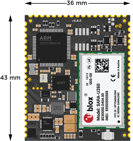
This diagram indicates only the dimensions; the components on the module will be different.
Dimensions and weight
- Width = 36 mm
- Height = 43 mm
- Thickness = 4.6 mm
- Weight = 8 gms
Recommended PCB land pattern
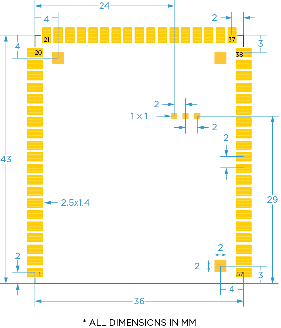
An E series part for EAGLE can be found in the Particle EAGLE library
Country compatibility
| Country | Model | Technologies | Carriers |
|---|---|---|---|
| Canada | E404 | M1 | Bell Mobility, Rogers Wireless, Telus |
| Mexico | E404 | M1 | AT&T |
| United States | E404 | M1 | AT&T |
Ordering information
To be provided at a later date
Product handling
ESD precautions
The E series contains highly sensitive electronic circuitry and is an Electrostatic Sensitive Device (ESD). Handling an E series without proper ESD protection may destroy or damage it permanently. Proper ESD handling and packaging procedures must be applied throughout the processing, handling and operation of any application that incorporates EØs. ESD precautions should be implemented on the application board where the E series is mounted. Failure to observe these precautions can result in severe damage to the E series!
Connectors
The U.FL antenna connectors are not designed to be constantly plugged and unplugged. The antenna pin is static sensitive and you can destroy the radio with improper handling. A tiny dab of glue (epoxy, liquid tape or hot glue) on the connector can be used securely hold the plug in place.
Default settings
The E series comes pre-programmed with a bootloader and a user application called Tinker. This application works with an iOS and Android app also named Tinker that allows you to very easily toggle digital pins, take analog and digital readings and drive variable PWM outputs.
The bootloader allows you to easily update the user application via several different methods, USB, OTA, Serial Y-Modem, and also internally via the Factory Reset procedure. All of these methods have multiple tools associated with them as well.
You may use the Particle Web IDE to code, compile and flash a user application OTA (Over The Air). Particle Workbench is a full-featured desktop IDE for Windows, Mac, and Linux based on VSCode and supports both cloud-based and local gcc-arm compiles. The Particle CLI provides a command-line interface for cloud-based compiles and flashing code over USB.
Glossary
| Term | Definition |
|---|---|
| SMPS | Switch Mode Power Supply |
| SIM | Subscriber Identity Module |
| RF | Radio Frequency |
| SMT | Surface Mount Technology (often associated with SMD which is a surface mount device). |
| LED | Light Emitting Diode |
| RGB LED | Red green and blue LEDs combined and diffused in one package. |
| USB | Universal Serial Bus |
| Quiescent current | Current consumed in the deepest sleep state. |
| FT | Five-tolerant; Refers to a pin being tolerant to 5V. |
| 3V3 | +3.3Volt; The regulated +3.3V supply rail. Also used to note a pin is only 3.3V tolerant. |
| PMIC | Power Management Integrated Circuit |
| LiPo | Lithium-ion Polymer Battery |
| GSM | Global System for Mobile Communications |
| CDMA | Code Division Multiple Access |
| OTA | Over The Air; describing how firmware is transferred to the device. |
| uC | Microcontroller |
FCC ISED warnings and end product labeling requirements
Federal Communication Commission Interference Statement This equipment has been tested and found to comply with the limits for a Class B digital device, pursuant to Part 15 of the FCC Rules. These limits are designed to provide reasonable protection against harmful interference in a residential installation. This equipment generates, uses and can radiate radio frequency energy and, if not installed and used in accordance with the instructions, may cause harmful interference to radio communications. However, there is no guarantee that interference will not occur in a particular installation. If this equipment does cause harmful interference to radio or television reception, which can be determined by turning the equipment off and on, the user is encouraged to try to correct the interference by one of the following measures:
- Reorient or relocate the receiving antenna.
- Increase the separation between the equipment and receiver.
- Connect the equipment into an outlet on a circuit different from that to which the receiver is connected.
- Consult the dealer or an experienced radio/TV technician for help.
FCC Caution: Any changes or modifications not expressly approved by the party responsible for compliance could void the user's authority to operate this equipment. This device complies with Part 15 of the FCC Rules. Operation is subject to the following two conditions:
- This device may not cause harmful interference, and
- This device must accept any interference received, including interference that may cause undesired operation.
FCC Radiation Exposure Statement: This equipment complies with FCC radiation exposure limits set forth for an uncontrolled environment. This transmitter module must not be co-located or operating in conjunction with any other antenna or transmitter. This End equipment should be installed and operated with a minimum distance of 20 centimeters between the radiator and your body.
IMPORTANT NOTE: In the event that these conditions can not be met (for example certain laptop configurations or co-location with another transmitter), then the FCC authorization is no longer considered valid and the FCC ID can not be used on the final product. In these circumstances, the OEM integrator will be responsible for re-evaluating the end product (including the transmitter) and obtaining a separate FCC authorization.
End Product Labeling The final end product must be labeled in a visible area with the following:
Contains FCC ID: 2AEMI-E404X
To be provided at a later date
Manual Information to the End User The OEM integrator has to be aware not to provide information to the end user regarding how to install or remove this RF module in the user’s manual of the end product which integrates this module.
Canada Statement This device complies with Industry Canada’s licence-exempt RSSs. Operation is subject to the following two conditions:
- This device may not cause interference; and
- This device must accept any interference, including interference that may cause undesired operation of the device.
Le présent appareil est conforme aux CNR d’Industrie Canada applicables aux appareils radio exempts de licence.
L’exploitation est autorisée aux deux conditions suivantes:
- l’appareil ne doit pas produire de brouillage;
- l’utilisateur de l’appareil doit accepter tout brouillage radioélectrique subi, même si le brouillage est susceptible d’en compromettre le fonctionnement.
Caution Exposure: This device meets the exemption from the routine evaluation limits in section 2.5 of RSS102 and users can obtain Canadian information on RF exposure and compliance. Le dispositif répond à l'exemption des limites d'évaluation de routine dans la section 2.5 de RSS102 et les utilisateurs peuvent obtenir des renseignements canadiens sur l'exposition aux RF et le respect.
The final end product must be labelled in a visible area with the following: The Industry Canada certification label of a module shall be clearly visible at all times when installed in the host device, otherwise the host device must be labelled to display the Industry Canada certification number of the module, preceded by the words “Contains transmitter module”, or the word “Contains”, or similar wording expressing the same meaning, as follows:
Contains transmitter module ISED: 20127-E404X
This End equipment should be installed and operated with a minimum distance of 20 centimeters between the radiator and your body. Cet équipement devrait être installé et actionné avec une distance minimum de 20 centimètres entre le radiateur et votre corps.
The end user manual shall include all required regulatory information/warning as shown in this manual.
For an in-depth review on certifications, please click here.
Revision history
| Revision | Date | Author | Comments |
|---|---|---|---|
| pre | 2022-01-25 | RK | Pre-release |
| 2022-03-14 | RK | Minor edits; no functional changes | |
| 2022-05-06 | RK | Wire1 is not exposed on C4/C5 | |
| 2022-07-28 | RK | Update PWM assignments | |
| 2022-09-08 | RK | Update antenna, FCC, and ISED | |
| 2022-09-16 | RK | Add minimum Device OS version, is 4.0.0 | |
| 2022-10-12 | RK | Removed power consumption section, was for B404 not E404X | |
| 2023-01-06 | RK | Update ADC information | |
| 2023-01-11 | RK | Updated certifications, added ISED, removed PTCRB | |
| 2023-01-17 | RK | Added FCC § 2.1033(b)(5) Block Diagram | |
| 2023-01-31 | RK | Add Device OS versions | |
| 1 | 2023-02-07 | RK | GA (remove preliminary banner) |
| 2 | 2023-02-17 | RK | Update certififed bands list |
| 3 | 2023-05-17 | RK | Fix maximum voltage on LI pin (pin 5) |
| 4 | 2024-01-03 | RK | Clarify use of PMID |
| 5 | 2024-03-19 | RK | Corrected LTE M1 band list |
Known errata
Contact
Web
Community Forums