
M-SoM from P2 migration guide
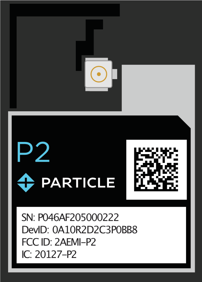 | 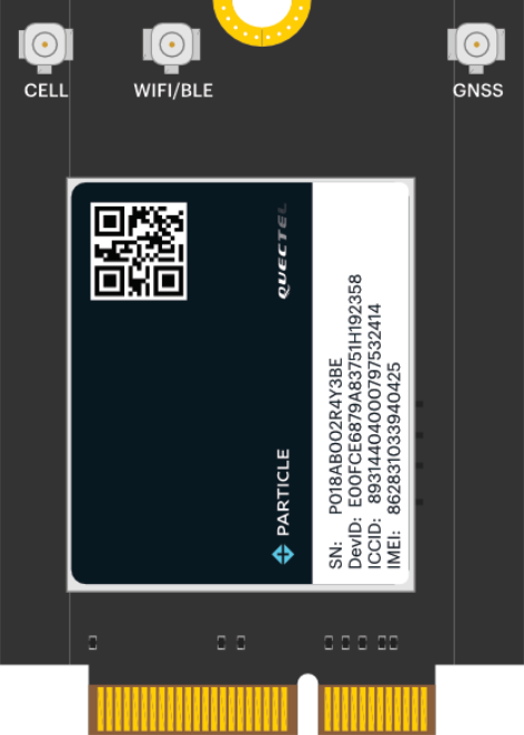 |
Pictures are not the same scale
The P2 module is a Wi-Fi SMD module that is mounted directly to your custom base board, while the M-SoM is a M.2 SoM that fits in a M.2 socket on your base board and has both cellular and Wi-Fi capabilities. The Particle M-SoM is larger and will not fit in the same footprint as the P2.
However, since the P2 has a Realtek RTL8721DM processor and the M-SoM has a Realtek RTL8722DM which is substantially similar, only having more GPIO, the migration should be relatively straightforward.
Datasheets
Certification
When migrating to a new device, recertification is typically required. If you are using the standard Particle antennas you often only need to complete the less expensive unintentional radiator testing of your completed assembly, however in some cases intentional radiator testing could be required.
Hardware
Antenna
The P2 has a choice between an internal trace antenna on the module or an external antenna for Wi-Fi and BLE (shared) connected by a U.FL connector.
The M-SoM requires an external antenna for cellular. It also requires a separate external antenna for Wi-Fi and BLE (shared). All antennas are connected by U.FL connectors.
Voltage regulators
The M-SoM has peak power usage that is higher than the P2. Be sure the check the guidelines below carefully.
As the M-SoM requires dual supply voltages, you may want to consider using the PM-BAT power module that includes the PMIC, fuel gauge, and voltage regulators.
VCC
VCC is used to supply power to the cellular module. The recommended input voltage range on this pin is between 3.6V to 4.2V DC. This can be connected directly to a 3.7V LiPo battery.
If you are not using a battery, or using a battery of a different voltage, you should use a regulator to supply 3.7V to 4.2V at 2A. You may want to add additional bulk capacitors to handle the short, high current peak usage when the cellular modem is transmitting.
The P2 does not require this voltage.
3V3
3V3 is used to supply power to MCU, Wi-Fi, BLE, logic ICs, memory, etc.. Make sure that the supply can handle a minimum of 500 mA.
These limits do not include any 3.3V peripherals on your base board, so that may increase the current requirements.
Power supply requirements:
- 3.3V output
- Maximum 5% voltage drop
- 100 mV peak-to-peak ripple maximum
- 500 mA minimum output current at 3.3V recommended for future compatibility
- Maintain these values at no-load as well as maximum load
In some cases, it may be necessary to add a supervisory/reset IC, such as the Richtek RT9818C or SG Micro SGM809-RXN3L/TR:
- If your power supply has a slew rate from 1.5V to 3.0V slower than 15 ms, a reset IC is required.
- If your power supply at power off cannot be guaranteed to drop below 0.3V before powering back up, a reset IC required.
See supervisory reset in the M-SoM datasheet, for additional information.
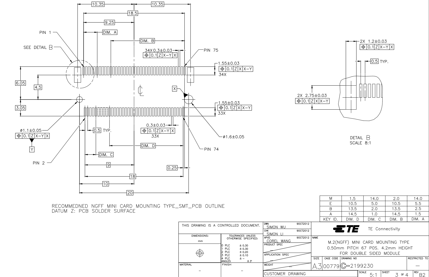
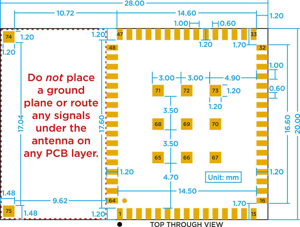
Land pattern
The land pattern for the M.2 connector on the M-SoM is:
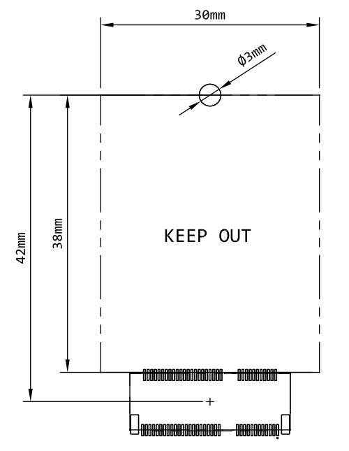
The P2 land pattern is:
ADC
| P2 Pin Name | P2 ADC | M-SoM Pin | M-SoM Pin Name | M-SoM ADC |
|---|---|---|---|---|
| A0 / D11 | ✓ | 23 | A0 / D19 | ✓ |
| A1 / D12 | ✓ | 33 | A1 / D18 | ✓ |
| A2 / D13 | ✓ | 35 | A2 / D17 | ✓ |
| A5 / D14 | ✓ | 43 | A5 / D14 | ✓ |
| 53 | A5 / D14 | ✓ | ||
| 45 | A6 / D29 | ✓ | ||
| 47 | A7 / WKP | ✓ | ||
| D0 / A3 | ✓ | 22 | D0 | |
| D1 / A4 | ✓ | 20 | D1 | |
| S0 / D15 | 41 | A4 / D15 | ✓ | |
| S1 / D16 | 37 | A3 / D16 | ✓ | |
| S2 / D17 | 35 | A2 / D17 | ✓ | |
| S3 / D18 | 33 | A1 / D18 | ✓ | |
| S4 / D19 | 23 | A0 / D19 | ✓ |
- 6 ADC on the M-SoM vs. 6 on the P2
- On the P2, 2 of the ADCs are on the same pins as I2C
- ADC inputs are single-ended and limited to 0 to 3.3V on both
- Resolution is 12 bits on both
- SoM pin 45 (A6) on the M-SoM is shared with SoM pin 53 (SWD_CLK). You cannot use A6 and SWD at the same time. If you implement SWD on your base board, driving pin A6 will prevent SWD from functioning. The SWD_CLK will be driven at hoot by the MCU.
- On the P2,
VBAT_MEASis a 5V tolerant ADC for measuring battery voltage. This is not present on the M-SoM as typically you will use a fuel gauge chip instead of the less accurate voltage measurement to measure battery SoC. - ADC input A7 has a low impedance which may be an issue when supplied from a voltage divider. The other ADC inputs are comparable to the P2/Photon 2.
Serial
| P2 Pin Name | P2 Serial | M-SoM Pin | M-SoM Pin Name | M-SoM Serial |
|---|---|---|---|---|
| D10 / WKP | Serial3 (CTS) | 38 | RX / D10 | Serial1 (RX) |
| S0 / D15 | Serial3 (TX) | 41 | A4 / D15 | |
| S1 / D16 | Serial3 (RX) | 37 | A3 / D16 | |
| S2 / D17 | Serial3 (RTS) | 35 | A2 / D17 | |
| D2 | Serial2 (RTS) | 42 | D2 | Serial1 (RTS) |
| 58 | D24 | Serial2 (TX) | ||
| 60 | D25 | Serial2 (RX) | ||
| D3 | Serial2 (CTS) | 40 | D3 | Serial1 (CTS) |
| D4 | Serial2 (TX) | 66 | D4 | |
| D5 | Serial2 (RX) | 68 | D5 | |
| RX / D9 | Serial1 (RX) | 36 | TX / D9 | Serial1 (TX) |
| TX / D8 | Serial1 (TX) | 36 | TX / D9 | Serial1 (TX) |
- The P2 has a third UART serial port; this does not exist on M-SoM
SPI
| P2 Pin Name | P2 SPI | M-SoM Pin | M-SoM Pin Name | M-SoM SPI |
|---|---|---|---|---|
| D10 / WKP | 38 | RX / D10 | SPI1 (MISO) | |
| S0 / D15 | SPI (MOSI) | 41 | A4 / D15 | |
| S1 / D16 | SPI (MISO) | 37 | A3 / D16 | |
| S2 / D17 | SPI (SCK) | 35 | A2 / D17 | |
| S3 / D18 | SPI (SS) | 33 | A1 / D18 | |
| D2 | SPI1 (MOSI) | 42 | D2 | SPI1 (SCK) |
| D3 | SPI1 (MISO) | 40 | D3 | SPI1 (SS) |
| D4 | SPI1 (SCK) | 66 | D4 | |
| D5 | SPI1 (SS) | 68 | D5 | |
| 48 | D8 | SPI (SS) | ||
| RX / D9 | 36 | TX / D9 | SPI1 (MOSI) | |
| 50 | MISO / D11 | SPI (MISO) | ||
| 52 | MOSI / D12 | SPI (MOSI) | ||
| 54 | SCK / D13 | SPI (SCK) | ||
| TX / D8 | 36 | TX / D9 | SPI1 (MOSI) |
- Two SPI interfaces on both
- SPI uses the RTL872x SPI0 peripheral (50 MHz maximum speed) on M-SoM
- SPI1 uses the RTL872x SPI1 peripheral (25 MHz maximum speed) on M-SoM
- Note: The P2/Photon 2 maximum speeds for SPI and SPI1 are reversed from the M-SoM
I2C
| P2 Pin Name | P2 I2C | M-SoM Pin | M-SoM Pin Name | M-SoM I2C |
|---|---|---|---|---|
| D0 / A3 | Wire (SDA) | 22 | D0 | Wire (SDA) |
| D1 / A4 | Wire (SCL) | 20 | D1 | Wire (SCL) |
- 1 I2C on both
- On the M-SoM (and P2 and Photon 2), the only valid I2C clock speeds are
CLOCK_SPEED_100KHZandCLOCK_SPEED_400KHZ. Other speeds are not supported at this time.
PWM
| P2 Pin Name | P2 PWM | M-SoM Pin | M-SoM Pin Name | M-SoM PWM |
|---|---|---|---|---|
| A0 / D11 | 23 | A0 / D19 | ✓ | |
| A1 / D12 | 33 | A1 / D18 | ✓ | |
| A2 / D13 | ✓ | 35 | A2 / D17 | |
| A5 / D14 | ✓ | 43 | A5 / D14 | ✓ |
| 53 | A5 / D14 | ✓ | ||
| 45 | A6 / D29 | ✓ | ||
| D1 / A4 | ✓ | 20 | D1 | |
| D10 / WKP | 38 | RX / D10 | ✓ | |
| S0 / D15 | ✓ | 41 | A4 / D15 | |
| S1 / D16 | ✓ | 37 | A3 / D16 | |
| S3 / D18 | 33 | A1 / D18 | ✓ | |
| S4 / D19 | 23 | A0 / D19 | ✓ | |
| D4 | 66 | D4 | ✓ | |
| D5 | 68 | D5 | ✓ | |
| D6 | 70 | D6 | ✓ | |
| D7 | 72 | D7 | ✓ | |
| RX / D9 | 36 | TX / D9 | ✓ | |
| 50 | MISO / D11 | ✓ | ||
| 52 | MOSI / D12 | ✓ | ||
| TX / D8 | 36 | TX / D9 | ✓ |
- PWM pins vary between the P2 and M-SoM
PDM
Pulse density modulation digital microphones can be used with the Microphone_PDM library and the M-SoM, but only on specific pins that are different from the P2!
| P2 Pin Name | P2 PDM | M-SoM Pin | M-SoM Pin Name | M-SoM PDM |
|---|---|---|---|---|
| A0 / D11 | CLK | 23 | A0 / D19 | |
| A1 / D12 | DAT | 33 | A1 / D18 | |
| S0 / D15 | 41 | A4 / D15 | DAT | |
| S1 / D16 | 37 | A3 / D16 | CLK |
Boot mode pins
These pins have a special function at boot. Beware when using these pins as input as they can trigger special modes in the MCU.
| Pin | Pin Name | Description | MCU |
|---|---|---|---|
| 43 | A5 / D14 | SWCLK. 40K pull-down at boot. | PB[3] |
| 53 | A5 / D14 | SWCLK. 40K pull-down at boot. | PB[3] |
| 55 | D27 | SWDIO. 40K pull-up at boot. Low at boot triggers MCU test mode. | PA[27] |
| 58 | D24 | Low at boot triggers ISP flash download | PA[7] |
| 60 | D25 | Goes high at boot | PA[8] |
| 61 | RGBR | Low at boot triggers trap mode | PA[30] |
Sleep
In
HIBERNATEsleep mode, the M-SoM and P2 can only be wakened by certain pinsThe
WKPpin is A7 the M-SoM (and B-SoM) but is pin D10 on the P2.In
HIBERNATEsleep mode, certain pins on the M-SoM and P2 do not preserveINPUT_PULLUPorINPUT_PULLDOWNwhile asleep. See details below.
M-SoM pins related to HIBERNATE sleep mode:
| Pin | Pin Name | Description | Interface | MCU |
|---|---|---|---|---|
| 36 | TX / D9 | Serial TX, PWM, GPIO, SPI1 MOSI, I2S MCLK | Pin can wake from HIBERNATE sleep | PA[12] |
| 38 | RX / D10 | Serial RX, PWM, GPIO, SPI1 MISO | Pin can wake from HIBERNATE sleep | PA[13] |
| 40 | D3 | D3 GPIO, Serial1 CTS flow control (optional), SPI1 SS | Pin can wake from HIBERNATE sleep | PA[15] |
| 42 | D2 | D2 GPIO, Serial RTS flow control (optional), SPI1 SCK | Pin can wake from HIBERNATE sleep | PA[14] |
| 47 | A7 / WKP | A7 Analog In, WKP, GPIO D28 | Pin can wake from HIBERNATE sleep | PA[20] |
| 48 | D8 | D8 GPIO, SPI SS | Pin can wake from HIBERNATE sleep | PA[19] |
| 50 | MISO / D11 | D11 GPIO, PWM, SPI MISO | Pin can wake from HIBERNATE sleep | PA[17] |
| 52 | MOSI / D12 | D12 GPIO, PWM, SPI MOSI | Pin can wake from HIBERNATE sleep | PA[16] |
| 54 | SCK / D13 | D13 GPIO, SPI SCK | Pin can wake from HIBERNATE sleep | PA[18] |
These P2 pins can wake from HIBERNATE sleep mode:
| Pin | Pin Name | Description | Interface | MCU |
|---|---|---|---|---|
| 30 | D10 / WKP | D10 GPIO, Serial 3 CTS, WKP. (Was WKP/A7 on P1.) | Pin can wake from HIBERNATE sleep | PA[15] |
| 40 | S0 / D15 | S0 GPIO, PWM, SPI MOSI, Serial3 TX, I2S MCLK. (Was P1S0 on P1.) | Pin can wake from HIBERNATE sleep | PA[12] |
| 41 | S1 / D16 | S1 GPIO, PWM, SPI MISO, Serial3 RX. (Was P1S1 on P1.) | Pin can wake from HIBERNATE sleep | PA[13] |
| 42 | S2 / D17 | S2 GPIO, SPI SCK, Serial3 RTS. (Was P1S2 on P1.) | Pin can wake from HIBERNATE sleep | PA[14] |
| 45 | D2 | D2 GPIO, Serial2 RTS, SPI1 MOSI | Pin can wake from HIBERNATE sleep | PA[16] |
| 51 | D3 | D3 GPIO, Serial2 CTS, SPI1 MISO | Pin can wake from HIBERNATE sleep | PA[17] |
| 52 | D4 | D4 GPIO, Serial2 TX, SPI1 SCK | Pin can wake from HIBERNATE sleep | PA[18] |
| 53 | D5 | D5 GPIO, Serial2 RX, SPI1 SS | Pin can wake from HIBERNATE sleep | PA[19] |
These P2 pins have special restrictions on using internal pull-up or pull-down while in HIBERNATE sleep mode. These
also cannot be used as wake from hibernate sleep pins.
| Pin | Pin Name | Description | Interface | MCU |
|---|---|---|---|---|
| 33 | S6 / D21 | S6 GPIO, I2S WS. (Was P1S6/TESTMODE on P1.) | No internal pull up or pull down in HIBERNATE sleep mode. | PB[31] |
| 47 | S4 / D19 | S4 GPIO, I2S RX. (Was P1S4 on P1.) | No internal pull up or pull down in HIBERNATE sleep mode. | PA[0] |
Full comparison
3V3
| P2 | M-SoM | ||
|---|---|---|---|
| Pin Name | 3V3 | 3V3 | |
| ∆ | Description | 3.3V power to MCU | System power in, supply a fixed 3.3V power, 500 mA minimum |
3V3_IO
| Removed from P2 | |
|---|---|
| Pin Name | 3V3_IO |
| Description | 3.3V power to MCU IO. |
3V3_RF
| Removed from P2 | |
|---|---|
| Pin Name | 3V3_RF |
| Description | 3.3V power to RF module |
A0
| P2 | M-SoM | ||
|---|---|---|---|
| Pin Name | A0 | A0 | |
| ∆ | Pin Alternate Name | D11 | D19 |
| ∆ | Description | A0 Analog in, PDM CLK, GPIO | A0 Analog in, GPIO, PWM |
| Supports digitalRead | Yes | Yes | |
| Supports digitalWrite | Yes | Yes | |
| Supports analogRead | Yes | Yes | |
| ∆ | Supports analogWrite (PWM) | No | Yes |
| ∆ | Supports tone | No | Yes |
| Supports attachInterrupt | Yes | Yes | |
| ∆ | Internal pull resistance | 2.1K | 42K |
A1
| P2 | M-SoM | ||
|---|---|---|---|
| Pin Name | A1 | A1 | |
| ∆ | Pin Alternate Name | D12 | D18 |
| ∆ | Description | A1 Analog in, PDM DAT, GPIO | A1 Analog in, GPIO, PWM |
| Supports digitalRead | Yes | Yes | |
| Supports digitalWrite | Yes | Yes | |
| Supports analogRead | Yes | Yes | |
| ∆ | Supports analogWrite (PWM) | No | Yes |
| ∆ | Supports tone | No | Yes |
| Supports attachInterrupt | Yes | Yes | |
| ∆ | Internal pull resistance | 2.1K | ??? |
A2
| P2 | M-SoM | ||
|---|---|---|---|
| Pin Name | A2 | A2 | |
| ∆ | Pin Alternate Name | D13 | D17 |
| ∆ | Description | A2 Analog in, PWM, GPIO | A2 Analog in, GPIO |
| Supports digitalRead | Yes | Yes | |
| Supports digitalWrite | Yes | Yes | |
| Supports analogRead | Yes | Yes | |
| ∆ | Supports analogWrite (PWM) | Yes | No |
| ∆ | Supports tone | Yes | No |
| Supports attachInterrupt | Yes | Yes | |
| ∆ | Internal pull resistance | 42K | 22K |
A5
| P2 | M-SoM | ||
|---|---|---|---|
| Pin Name | A5 | A5 | |
| Pin Alternate Name | D14 | D14 | |
| ∆ | Description | A5 Analog in, GPIO, PWM. | A5 Analog in, PWM, GPIO, shared with pin 53 |
| Supports digitalRead | Yes | Yes | |
| Supports digitalWrite | Yes | Yes | |
| Supports analogRead | Yes | Yes | |
| Supports analogWrite (PWM) | Yes | Yes | |
| Supports tone | Yes | Yes | |
| Supports attachInterrupt | Yes | Yes | |
| ∆ | Internal pull resistance | 42K | ??? |
| ∆ | SWD interface | n/a | SWCLK. 40K pull-down at boot. |
| ∆ | Signal used at boot | n/a | SWCLK. 40K pull-down at boot. |
A5
| Added to M-SoM | |
|---|---|
| Pin Name | A5 |
| Pin Alternate Name | D14 |
| Description | A5 Analog in, PWM, GPIO, SWCLK, shared with pin 43 |
| Supports digitalRead | Yes |
| Supports digitalWrite | Yes |
| Supports analogRead | Yes |
| Supports analogWrite (PWM) | Yes |
| Supports tone | Yes |
| Supports attachInterrupt | Yes |
| Internal pull resistance | 42K |
| SWD interface | SWCLK. 40K pull-down at boot. |
| Signal used at boot | SWCLK. 40K pull-down at boot. |
A6
| Added to M-SoM | |
|---|---|
| Pin Name | A6 |
| Pin Alternate Name | D29 |
| Description | A6 Analog in, GPIO, PWM, M.2 eval PMIC INT |
| Supports digitalRead | Yes |
| Supports digitalWrite | Yes |
| Supports analogRead | Yes |
| Supports analogWrite (PWM) | Yes |
| Supports tone | Yes |
| Supports attachInterrupt | Yes |
| Internal pull resistance | ??? |
A7
| Added to M-SoM | |
|---|---|
| Pin Name | A7 |
| Pin Alternate Name | WKP |
| Description | A7 Analog In, WKP, GPIO D28 |
| Supports digitalRead | Yes |
| Supports digitalWrite | Yes |
| Supports analogRead | Yes |
| Supports attachInterrupt | Yes |
| Internal pull resistance | ??? |
AGND
| Added to M-SoM | |
|---|---|
| Pin Name | AGND |
| Description | Analog Ground. |
CELL USBD-
| Added to M-SoM | |
|---|---|
| Pin Name | CELL USBD- |
| Description | Cellular Modem USB Data- |
| Input is 5V Tolerant | Yes |
CELL USBD+
| Added to M-SoM | |
|---|---|
| Pin Name | CELL USBD+ |
| Description | Cellular Modem USB Data+ |
| Input is 5V Tolerant | Yes |
CELL VBUS
| Added to M-SoM | |
|---|---|
| Pin Name | CELL VBUS |
| Description | USB detect pin for cellular modem. 5V on this pin enables the Cellular Modem USB interface. |
| Input is 5V Tolerant | Yes |
CELL_RI
| Added to M-SoM | |
|---|---|
| Pin Name | CELL_RI |
| Description | CELL_RI, ring indicator output, leave unconnected. |
D0
| P2 | M-SoM | ||
|---|---|---|---|
| Pin Name | D0 | D0 | |
| ∆ | Pin Alternate Name | A3 | n/a |
| ∆ | Description | D0 GPIO, I2C SDA, A3 Analog In | D0 GPIO, I2C SDA |
| Supports digitalRead | Yes | Yes | |
| Supports digitalWrite | Yes | Yes | |
| ∆ | Supports analogRead | Yes | No |
| I2C interface | SDA. Use Wire object. Use 1.5K to 10K external pull-up resistor. | SDA. Use Wire object. Use 1.5K to 10K external pull-up resistor. | |
| Supports attachInterrupt | Yes | Yes | |
| ∆ | Internal pull resistance | 22K | ??? |
D1
| P2 | M-SoM | ||
|---|---|---|---|
| Pin Name | D1 | D1 | |
| ∆ | Pin Alternate Name | A4 | n/a |
| ∆ | Description | D1 GPIO, PWM, I2C SCL, A4 Analog In | D1 GPIO, I2C SCL |
| Supports digitalRead | Yes | Yes | |
| Supports digitalWrite | Yes | Yes | |
| ∆ | Supports analogRead | Yes | No |
| ∆ | Supports analogWrite (PWM) | Yes | No |
| ∆ | Supports tone | Yes | No |
| I2C interface | SCL. Use Wire object. Use 1.5K to 10K external pull-up resistor. | SCL. Use Wire object. Use 1.5K to 10K external pull-up resistor. | |
| Supports attachInterrupt | Yes | Yes | |
| ∆ | Internal pull resistance | 22K | ??? |
D10
| P2 | M-SoM | ||
|---|---|---|---|
| ∆ | Pin Name | D10 | RX |
| ∆ | Pin Alternate Name | WKP | D10 |
| ∆ | Description | D10 GPIO, Serial 3 CTS, WKP. (Was WKP/A7 on P1.) | Serial RX, PWM, GPIO, SPI1 MISO |
| Supports digitalRead | Yes | Yes | |
| Supports digitalWrite | Yes | Yes | |
| ∆ | Supports analogWrite (PWM) | No | Yes |
| ∆ | Supports tone | No | Yes |
| ∆ | UART serial | CTS. Use Serial3 object. Flow control optional. | RX. Use Serial1 object. |
| ∆ | SPI interface | n/a | MISO. Use SPI1 object. |
| Supports attachInterrupt | Yes | Yes | |
| Internal pull resistance | 2.1K | 2.1K |
D15
| P2 | M-SoM | ||
|---|---|---|---|
| ∆ | Pin Name | S0 | A4 |
| Pin Alternate Name | D15 | D15 | |
| ∆ | Description | S0 GPIO, PWM, SPI MOSI, Serial3 TX, I2S MCLK. (Was P1S0 on P1.) | A4 Analog in, PDM DAT, GPIO |
| Supports digitalRead | Yes | Yes | |
| Supports digitalWrite | Yes | Yes | |
| ∆ | Supports analogRead | No | Yes |
| ∆ | Supports analogWrite (PWM) | Yes | No |
| ∆ | Supports tone | Yes | No |
| ∆ | UART serial | TX. Use Serial3 object. | n/a |
| ∆ | SPI interface | MOSI. Use SPI object. | n/a |
| Supports attachInterrupt | Yes | Yes | |
| ∆ | I2S interface | I2S MCLK | n/a |
| Internal pull resistance | 2.1K | 2.1K |
D16
| P2 | M-SoM | ||
|---|---|---|---|
| ∆ | Pin Name | S1 | A3 |
| Pin Alternate Name | D16 | D16 | |
| ∆ | Description | S1 GPIO, PWM, SPI MISO, Serial3 RX. (Was P1S1 on P1.) | A3 Analog in, PDM CLK, GPIO |
| Supports digitalRead | Yes | Yes | |
| Supports digitalWrite | Yes | Yes | |
| ∆ | Supports analogRead | No | Yes |
| ∆ | Supports analogWrite (PWM) | Yes | No |
| ∆ | Supports tone | Yes | No |
| ∆ | UART serial | RX. Use Serial3 object. | n/a |
| ∆ | SPI interface | MISO. Use SPI object. | n/a |
| Supports attachInterrupt | Yes | Yes | |
| Internal pull resistance | 2.1K | 2.1K |
D17
| P2 | M-SoM | ||
|---|---|---|---|
| ∆ | Pin Name | S2 | A2 |
| Pin Alternate Name | D17 | D17 | |
| ∆ | Description | S2 GPIO, SPI SCK, Serial3 RTS. (Was P1S2 on P1.) | A2 Analog in, GPIO |
| Supports digitalRead | Yes | Yes | |
| Supports digitalWrite | Yes | Yes | |
| ∆ | Supports analogRead | No | Yes |
| ∆ | UART serial | RTS. Use Serial3 object. Flow control optional. | n/a |
| ∆ | SPI interface | SCK. Use SPI object. | n/a |
| Supports attachInterrupt | Yes | Yes | |
| ∆ | Internal pull resistance | 2.1K | 22K |
D18
| P2 | M-SoM | ||
|---|---|---|---|
| ∆ | Pin Name | S3 | A1 |
| Pin Alternate Name | D18 | D18 | |
| ∆ | Description | S3 GPIO, I2S TX. (Was P1S3 on P1.), SPI SS | A1 Analog in, GPIO, PWM |
| Supports digitalRead | Yes | Yes | |
| Supports digitalWrite | Yes | Yes | |
| ∆ | Supports analogRead | No | Yes |
| ∆ | Supports analogWrite (PWM) | No | Yes |
| ∆ | Supports tone | No | Yes |
| ∆ | SPI interface | Default SS for SPI. | n/a |
| Supports attachInterrupt | Yes | Yes | |
| ∆ | I2S interface | I2S TX | n/a |
| ∆ | Internal pull resistance | 2.1K | ??? |
D19
| P2 | M-SoM | ||
|---|---|---|---|
| ∆ | Pin Name | S4 | A0 |
| Pin Alternate Name | D19 | D19 | |
| ∆ | Description | S4 GPIO, I2S RX. (Was P1S4 on P1.) | A0 Analog in, GPIO, PWM |
| Supports digitalRead | Yes | Yes | |
| Supports digitalWrite | Yes | Yes | |
| ∆ | Supports analogRead | No | Yes |
| ∆ | Supports analogWrite (PWM) | No | Yes |
| ∆ | Supports tone | No | Yes |
| Supports attachInterrupt | Yes | Yes | |
| ∆ | I2S interface | I2S RX | n/a |
| ∆ | Internal pull resistance | 22K. No internal pull up or pull down in HIBERNATE sleep mode. | 42K |
D2
| P2 | M-SoM | ||
|---|---|---|---|
| Pin Name | D2 | D2 | |
| ∆ | Description | D2 GPIO, Serial2 RTS, SPI1 MOSI | D2 GPIO, Serial RTS flow control (optional), SPI1 SCK |
| Supports digitalRead | Yes | Yes | |
| Supports digitalWrite | Yes | Yes | |
| ∆ | UART serial | RTS. Use Serial2 object. Flow control optional. | RTS. Use Serial1 object. |
| ∆ | SPI interface | MOSI. Use SPI1 object. | SCK. Use SPI1 object. |
| Supports attachInterrupt | Yes | Yes | |
| ∆ | Internal pull resistance | 2.1K | ??? |
D22
| Added to M-SoM | |
|---|---|
| Pin Name | D22 |
| Description | D22 GPIO |
| Supports digitalRead | Yes |
| Supports digitalWrite | Yes |
| Supports attachInterrupt | Yes |
| Internal pull resistance | ??? |
D23
| Added to M-SoM | |
|---|---|
| Pin Name | D23 |
| Description | D23 GPIO |
| Supports digitalRead | Yes |
| Supports digitalWrite | Yes |
| Supports attachInterrupt | Yes |
| Internal pull resistance | ??? |
D24
| Added to M-SoM | |
|---|---|
| Pin Name | D24 |
| Description | D24 GPIO, Serial2 TX, do not pull down at boot |
| Supports digitalRead | Yes |
| Supports digitalWrite | Yes |
| UART serial | TX. Use Serial2 object. |
| Supports attachInterrupt | Yes |
| Internal pull resistance | 42K |
| Signal used at boot | Low at boot triggers ISP flash download |
D25
| Added to M-SoM | |
|---|---|
| Pin Name | D25 |
| Description | GPIO25, Serial2 RX |
| Supports digitalRead | Yes |
| Supports digitalWrite | Yes |
| UART serial | RX. Use Serial2 object. |
| Supports attachInterrupt | Yes |
| Internal pull resistance | 42K |
| Signal used at boot | Goes high at boot |
D26
| Added to M-SoM | |
|---|---|
| Pin Name | D26 |
| Description | D26 GPIO, I2S WS |
| Supports digitalRead | Yes |
| Supports digitalWrite | Yes |
| Supports attachInterrupt | Yes |
| I2S interface | I2S WS |
| Internal pull resistance | ??? |
D27
| Added to M-SoM | |
|---|---|
| Pin Name | D27 |
| Description | D27 GPIO, SWDIO (SWD_DATA), do not pull down at boot |
| Supports digitalRead | Yes |
| Supports digitalWrite | Yes |
| Supports attachInterrupt | Yes |
| Internal pull resistance | 42K |
| SWD interface | SWDIO. 40K pull-up at boot. |
| Signal used at boot | SWDIO. 40K pull-up at boot. Low at boot triggers MCU test mode. |
D3
| P2 | M-SoM | ||
|---|---|---|---|
| Pin Name | D3 | D3 | |
| ∆ | Description | D3 GPIO, Serial2 CTS, SPI1 MISO | D3 GPIO, Serial1 CTS flow control (optional), SPI1 SS |
| Supports digitalRead | Yes | Yes | |
| Supports digitalWrite | Yes | Yes | |
| ∆ | UART serial | CTS. Use Serial2 object. Flow control optional. | CTS. Use Serial1 object. |
| ∆ | SPI interface | MISO. Use SPI1 object. | SS. Use SPI1 object. |
| Supports attachInterrupt | Yes | Yes | |
| ∆ | Internal pull resistance | 2.1K | ??? |
D4
| P2 | M-SoM | ||
|---|---|---|---|
| Pin Name | D4 | D4 | |
| ∆ | Description | D4 GPIO, Serial2 TX, SPI1 SCK | D4 GPIO, PWM |
| Supports digitalRead | Yes | Yes | |
| Supports digitalWrite | Yes | Yes | |
| ∆ | Supports analogWrite (PWM) | No | Yes |
| ∆ | Supports tone | No | Yes |
| ∆ | UART serial | TX. Use Serial2 object. | n/a |
| ∆ | SPI interface | SCK. Use SPI1 object. | n/a |
| Supports attachInterrupt | Yes | Yes | |
| ∆ | Internal pull resistance | 2.1K | ??? |
D5
| P2 | M-SoM | ||
|---|---|---|---|
| Pin Name | D5 | D5 | |
| ∆ | Description | D5 GPIO, Serial2 RX, SPI1 SS | D5 GPIO, PWM, I2S TX |
| Supports digitalRead | Yes | Yes | |
| Supports digitalWrite | Yes | Yes | |
| ∆ | Supports analogWrite (PWM) | No | Yes |
| ∆ | Supports tone | No | Yes |
| ∆ | UART serial | RX. Use Serial2 object. | n/a |
| ∆ | SPI interface | SS. Use SPI1 object. Can use any pin for SPI1 SS/CS however. | n/a |
| Supports attachInterrupt | Yes | Yes | |
| ∆ | I2S interface | n/a | I2S TX |
| ∆ | Internal pull resistance | 2.1K | ??? |
D6
| P2 | M-SoM | ||
|---|---|---|---|
| Pin Name | D6 | D6 | |
| ∆ | Description | D6 GPIO, SWCLK | D6 GPIO, PWM, I2S CLK |
| Supports digitalRead | Yes | Yes | |
| Supports digitalWrite | Yes | Yes | |
| ∆ | Supports analogWrite (PWM) | No | Yes |
| ∆ | Supports tone | No | Yes |
| Supports attachInterrupt | Yes | Yes | |
| ∆ | I2S interface | n/a | I2S CLK |
| ∆ | Internal pull resistance | 42K | ??? |
| ∆ | SWD interface | SWCLK. 40K pull-down at boot. | n/a |
| ∆ | Signal used at boot | SWCLK. 40K pull-down at boot. | n/a |
D7
| P2 | M-SoM | ||
|---|---|---|---|
| Pin Name | D7 | D7 | |
| ∆ | Description | D7 GPIO, SWDIO | D7 GPIO, PWM, I2S WS |
| ∆ | Supports digitalRead | Yes. | Yes |
| ∆ | Supports digitalWrite | Yes. On the Photon this is the blue D7 LED. | Yes |
| ∆ | Supports analogWrite (PWM) | No | Yes |
| ∆ | Supports tone | No | Yes |
| Supports attachInterrupt | Yes | Yes | |
| ∆ | I2S interface | n/a | I2S WS |
| ∆ | Internal pull resistance | 42K | ??? |
| ∆ | SWD interface | SWDIO. 40K pull-up at boot. | n/a |
| ∆ | Signal used at boot | SWDIO. 40K pull-up at boot. Low at boot triggers MCU test mode. | n/a |
D8
| Added to M-SoM | |
|---|---|
| Pin Name | D8 |
| Description | D8 GPIO, SPI SS |
| Supports digitalRead | Yes |
| Supports digitalWrite | Yes |
| SPI interface | Default SS for SPI. |
| Supports attachInterrupt | Yes |
| Internal pull resistance | 2.1K |
D9
| P2 | M-SoM | ||
|---|---|---|---|
| ∆ | Pin Name | RX | TX |
| Pin Alternate Name | D9 | D9 | |
| ∆ | Description | Serial1 RX (received data), GPIO | Serial TX, PWM, GPIO, SPI1 MOSI, I2S MCLK |
| Supports digitalRead | Yes | Yes | |
| Supports digitalWrite | Yes | Yes | |
| ∆ | Supports analogWrite (PWM) | No | Yes |
| ∆ | Supports tone | No | Yes |
| ∆ | UART serial | RX. Use Serial1 object. | TX. Use Serial1 object. |
| ∆ | SPI interface | n/a | MOSI. Use SPI1 object. |
| Supports attachInterrupt | Yes | Yes | |
| ∆ | I2S interface | n/a | I2S MCLK |
| ∆ | Internal pull resistance | 42K | 2.1K |
GND
| P2 | M-SoM | ||
|---|---|---|---|
| Pin Name | GND | GND | |
| ∆ | Description | Ground. Be sure you connect all P1 ground pins. | Ground. |
GNSS_TX
| Added to M-SoM | |
|---|---|
| Pin Name | GNSS_TX |
| Description | Cellular modem GNSS UART TX |
MISO
| Added to M-SoM | |
|---|---|
| Pin Name | MISO |
| Pin Alternate Name | D11 |
| Description | D11 GPIO, PWM, SPI MISO |
| Supports digitalRead | Yes |
| Supports digitalWrite | Yes |
| Supports analogWrite (PWM) | Yes |
| Supports tone | Yes |
| SPI interface | MISO. Use SPI object. |
| Supports attachInterrupt | Yes |
| Internal pull resistance | 2.1K |
MODE
| Unchanged between P2 and M-SoM | |
|---|---|
| Pin Name | MODE |
| Description | MODE button. Pin number constant is BTN. External pull-up required! |
| Supports attachInterrupt | Yes |
MOSI
| Added to M-SoM | |
|---|---|
| Pin Name | MOSI |
| Pin Alternate Name | D12 |
| Description | D12 GPIO, PWM, SPI MOSI |
| Supports digitalRead | Yes |
| Supports digitalWrite | Yes |
| Supports analogWrite (PWM) | Yes |
| Supports tone | Yes |
| SPI interface | MOSI. Use SPI object. |
| Supports attachInterrupt | Yes |
| Internal pull resistance | 2.1K |
NC
| P2 | M-SoM | ||
|---|---|---|---|
| Pin Name | NC | NC | |
| ∆ | Description | No connection. Do not connect anything to this pin. | n/a |
RGBB
| P2 | M-SoM | ||
|---|---|---|---|
| Pin Name | RGBB | RGBB | |
| Description | RGB LED Blue | RGB LED Blue | |
| ∆ | Supports attachInterrupt | Yes | No |
RGBG
| P2 | M-SoM | ||
|---|---|---|---|
| Pin Name | RGBG | RGBG | |
| Description | RGB LED Green | RGB LED Green | |
| ∆ | Supports attachInterrupt | Yes | No |
RGBR
| P2 | M-SoM | ||
|---|---|---|---|
| Pin Name | RGBR | RGBR | |
| ∆ | Description | RGB LED Red. Has 10K hardware pull-up. Do not hold low at boot. | RGB LED Red |
| ∆ | Supports attachInterrupt | Yes | No |
| ∆ | Signal used at boot | n/a | Low at boot triggers trap mode |
RST
| P2 | M-SoM | ||
|---|---|---|---|
| Pin Name | RST | RST | |
| ∆ | Description | Hardware reset. Pull low to reset; can leave unconnected in normal operation. | Hardware reset, active low. External pull-up required. |
S5
| P2 | M-SoM | ||
|---|---|---|---|
| ∆ | Pin Name | S5 | D20 |
| ∆ | Pin Alternate Name | D20 | n/a |
| ∆ | Description | S5 GPIO, I2S CLK. (Was P1S5 on P1.) | D20 GPIO, I2S TX |
| ∆ | Supports digitalRead | No | Yes |
| Supports digitalWrite | Yes | Yes | |
| Supports attachInterrupt | Yes | Yes | |
| ∆ | I2S interface | I2S CLK | I2S TX |
| ∆ | Internal pull resistance | 22K. No internal pull up or pull down in HIBERNATE sleep mode | ??? |
S6
| P2 | M-SoM | ||
|---|---|---|---|
| ∆ | Pin Name | S6 | D21 |
| ∆ | Pin Alternate Name | D21 | n/a |
| ∆ | Description | S6 GPIO, I2S WS. (Was P1S6/TESTMODE on P1.) | D21 GPIO, I2S RX |
| Supports digitalRead | Yes | Yes | |
| Supports digitalWrite | Yes | Yes | |
| Supports attachInterrupt | Yes | Yes | |
| ∆ | I2S interface | I2S WS | I2S RX |
| Internal pull resistance | 22K. No internal pull up or pull down in HIBERNATE sleep mode. | 22K. No internal pull up or pull down in HIBERNATE sleep mode. |
SCK
| Added to M-SoM | |
|---|---|
| Pin Name | SCK |
| Pin Alternate Name | D13 |
| Description | D13 GPIO, SPI SCK |
| Supports digitalRead | Yes |
| Supports digitalWrite | Yes |
| SPI interface | SCK. Use SPI object. |
| Supports attachInterrupt | Yes |
| Internal pull resistance | 2.1K |
SIM_CLK
| Added to M-SoM | |
|---|---|
| Pin Name | SIM_CLK |
| Description | Leave unconnected, 1.8V/3V SIM Clock Output from cellular modem. |
SIM_DATA
| Added to M-SoM | |
|---|---|
| Pin Name | SIM_DATA |
| Description | Leave unconnected, 1.8V/3V SIM Data I/O of cellular modem with internal 4.7 k pull-up. |
SIM_RST
| Added to M-SoM | |
|---|---|
| Pin Name | SIM_RST |
| Description | Leave unconnected, 1.8V/3V SIM Reset Output from cellular modem. |
SIM_VCC
| Added to M-SoM | |
|---|---|
| Pin Name | SIM_VCC |
| Description | Leave unconnected, 1.8V/3V SIM Supply Output from R410M. |
TX
| P2 | M-SoM | ||
|---|---|---|---|
| Pin Name | TX | TX | |
| ∆ | Pin Alternate Name | D8 | D9 |
| ∆ | Description | Serial1 TX (transmitted data), GPIO | Serial TX, PWM, GPIO, SPI1 MOSI, I2S MCLK |
| Supports digitalRead | Yes | Yes | |
| Supports digitalWrite | Yes | Yes | |
| ∆ | Supports analogWrite (PWM) | No | Yes |
| ∆ | Supports tone | No | Yes |
| UART serial | TX. Use Serial1 object. | TX. Use Serial1 object. | |
| ∆ | SPI interface | n/a | MOSI. Use SPI1 object. |
| Supports attachInterrupt | Yes | Yes | |
| ∆ | I2S interface | n/a | I2S MCLK |
| ∆ | Internal pull resistance | 42K | 2.1K |
| ∆ | Signal used at boot | Low at boot triggers ISP flash download | n/a |
USBDATA-
| Unchanged between P2 and M-SoM | |
|---|---|
| Pin Name | USBDATA- |
| Description | USB Data- |
| Input is 5V Tolerant | Yes |
USBDATA+
| Unchanged between P2 and M-SoM | |
|---|---|
| Pin Name | USBDATA+ |
| Description | USB Data+ |
| Input is 5V Tolerant | Yes |
VBAT_MEAS
| Removed from P2 | |
|---|---|
| Pin Name | VBAT_MEAS |
| Description | Battery voltage measurement (optional). |
| Input is 5V Tolerant | Yes |
VCC
| Added to M-SoM | |
|---|---|
| Pin Name | VCC |
| Description | System power in, connect to the +LiPo or supply a fixed 3.6-4.3V power. |
Software
Wi-Fi configuration
Wi-Fi setup works the same as the P2, Photon 2, and Argon, and uses BLE. See Wi-Fi setup options for more information.
Platform ID
The Platform ID of the msom (35, PLATFORM_MSOM) is different from that of the P2 (32) because of the different hardware.
If you have a product based on the P2, you will need to create a separate product for devices using the M-SoM. While you may be able to use the same source code to build your application, the firmware binaries uploaded to the console will be different, so they need to be separate products. This generally does not affect billing as only the number of devices, not the number of products, is counted toward your plan limits.
Third-party libraries
Most third-party libraries are believed to be compatible between the P2 and M-SoM as they share a similar MCU. The exceptions include:
- Libraries that are hardcoded to support only certain platforms by their PLATFORM_ID
Revision history
| Revision | Date | Author | Comments |
|---|---|---|---|
| pre | 2023-10-03 | RK | Initial version |
| 2023-12-20 | RK | Additional notes for ADCs, D24, and D25 | |
| 001 | 2024-04-02 | RK | General availability |
| 002 | 2024-04-18 | RK | Add PDM microphone |
| 003 | 2025-01-07 | RK | Added power supply notes |