
M-SoM datasheet
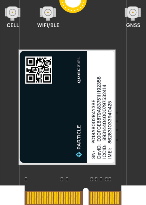
Overview
The Particle M-SoM contains the following functional units:
- M.2 SoM form-factor, like the B-Series SoM
- Can use cellular or Wi-Fi (2.4 GHz or 5 GHz) for the cloud connection
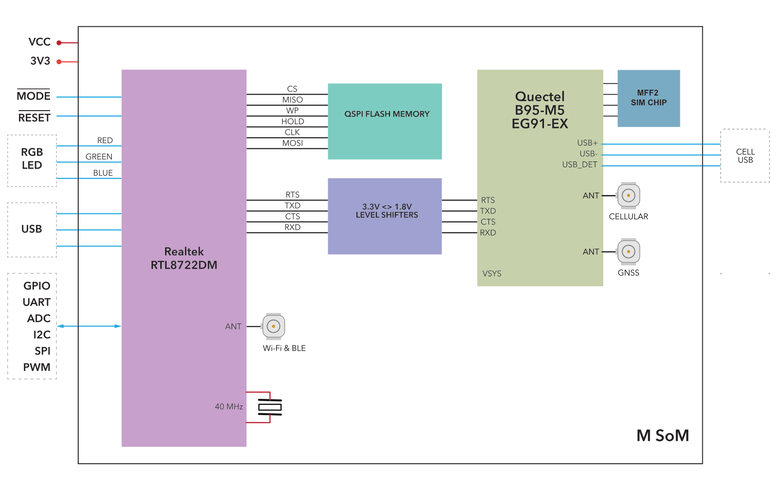
- Realtek RTL8722DM MCU (BLE and Wi-Fi)
- Cellular modem
- M404: Quectel BG95-M5 LTE Cat M1 (NorAm)
- M524: Quectel EG91-EX LTE Cat 1 with 2G/3G fallback (EMEAA)
- M635e: Quectel BG95-S5 LTE Cat M1/2G (Global with NTN satellite)
MCU
The Realtek RTL8722DM is in the same family as the P2 and Photon 2 modules (RTL8721DM), but has additional GPIO.
- 802.11a/b/g/n Wi-Fi, 2.4 GHz and 5 GHz
- U.FL connector for external antenna
- BLE 5 using same antenna as Wi-Fi
- Realtek RTL8722DM MCU
- ARM Cortex M33 CPU, 200 MHz
- 2048 KB (2 MB) user application maximum size
- 3072 KB (3 MB) of RAM available to user applications
- 8 MB flash file system
- FCC (United States), ISED (Canada), and CE (European Union) certified
Block diagram
Device families
| Cellular Only | Cellular & Wi-Fi | Wi-Fi Only | |
|---|---|---|---|
| Developer devices | Boron | Photon 2 | |
| Production module | B-SoM | M-SoM | P2 |
Migration guides
If you are migrating to the M-SoM from another Particle device, see also the following migration guides:
Power
VCC
VCC (sometimes referred to as 3V7) is used to supply power to the cellular module. The recommended input voltage range on this pin is between 3.6V to 4.2V DC. This can be connected directly to a 3.7V LiPo battery. Make sure that the supply can handle currents of at least 2 A.
If you are not using a battery, or using a battery of a different voltage, you should use a regulator to supply 3.7V to 4.2V at 2A. You may want to add additional bulk capacitors to handle the short, high current peak usage when the cellular modem is transmitting.
Note:
It is highly recommended that you design your power supply to the full 2A maximum current even though the M404 (LTE Cat M1) does not use the full amount.
Other models, including the M524 and M635e, support 2G cellular, which uses significantly more current than LTE Cat M1 or Cat 1, and also takes much longer to connect, which may affect battery life.
3V3
3V3 is used to supply power to RTL8722 MCU, logic ICs, memory, etc.. Make sure that the supply can handle a minimum of 500 mA.
These limits do not include any 3.3V peripherals on your base board, so that may increase the current requirements.
Power supply requirements:
- 3.3V output
- Maximum 5% voltage drop
- 100 mV peak-to-peak ripple maximum
- 500 mA minimum output current at 3.3V recommended for future compatibility
- Maintain these values at no-load as well as maximum load
In some cases, it may be necessary to add a supervisory/reset IC, such as the Richtek RT9818C or SG Micro SGM809-RXN3L/TR:
- If your power supply has a slew rate from 1.5V to 3.0V slower than 15 ms, a reset IC is required.
- If your power supply at power off cannot be guaranteed to drop below 0.3V before powering back up, a reset IC required.
See supervisory reset, below, for additional information.
RF
The M-SoM includes three U.FL connectors for external antennas:
- Cellular
- Wi-Fi (2.4 GHz and 5 GHz) and BLE
- GNSS (GPS)
Wi-Fi operation in the 5150-5250 MHz band is only for indoor use to reduce the potential for harmful interference to co-channel mobile satellite systems.
Approved Antennas
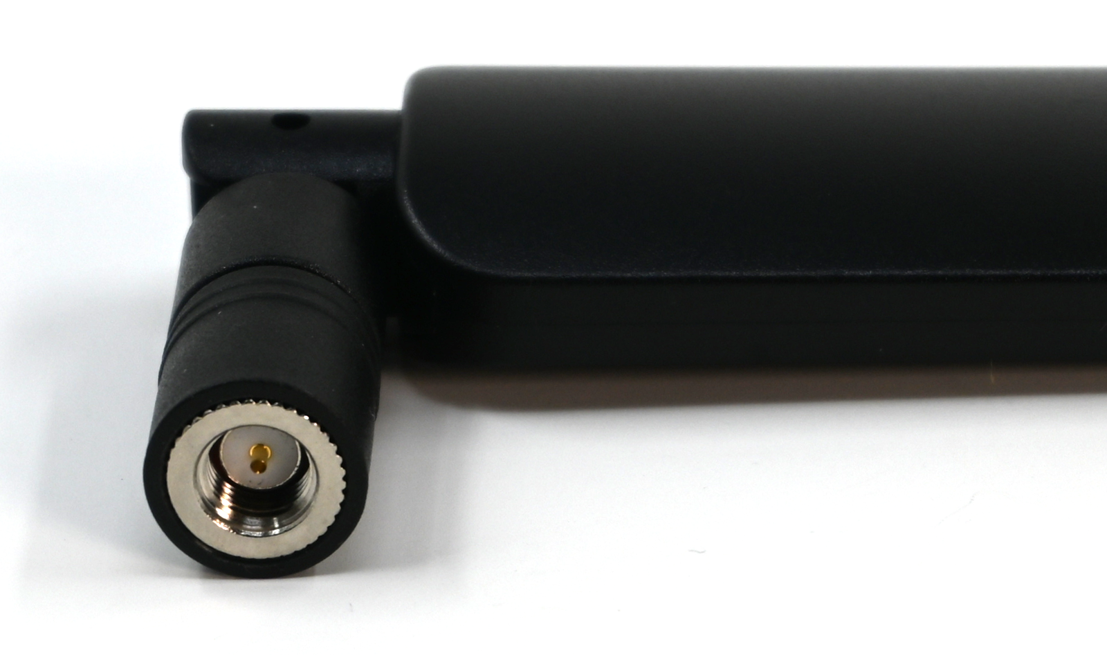
Certified cellular antennas
The M-SoM is certified with the following cellular antenna:
| Antenna | SKU | Details | Links |
|---|---|---|---|
| Wide band LTE cell antenna [x1] | PARANTCW1EA | B504e and M-SoM | Datasheet |
| Wide band LTE cell antenna [x50] | PARANTCW1TY | B504e and M-SoM | Datasheet |
Single quantity units and developer kits include a PARANTCW1EA antenna. Tray quantities of the do not include antennas.
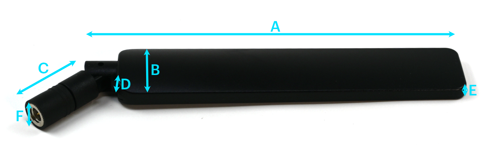
| Dimension | Value | Unit |
|---|---|---|
| Length | 116.0 | mm |
| Width | 27.0 | mm |
| Thickness | 0.2 | mm |
| Cable Length | 189.5 | mm |
| Parameter | 617-960 | 1156 - 1496 | 1520 - 1660.5 | 1710 - 2700 | 3330 - 4200 | 4200 - 5925 |
|---|---|---|---|---|---|---|
| V.S.W.R. | ≤ 3.5 | ≤ 3.0 | ≤ 2.0 | ≤ 2.0 | ≤ 1.5 | ≤ 2.0 |
| Peak Gain | 2.8 dBi | 2.4 dBi | 3.9 dBi | 5.3 dBi | 5.6 dBi | 7.9 dBi |
| Eff % (max/avg) | 71/62 | 55/53 | 68/62 | 85/70 | 76/71 | 69/62 |
Certified Wi-Fi/BLE antennas
The M-SoM is certified for use with the same antennas as the P2/Photon 2. The same antenna is shared for Wi-Fi and BLE. Unlike the P2/Photon 2, the external antenna is required for Wi-Fi and BLE and the M-SoM does not include a built-in trace antenna on the module.
| Antenna | SKU | Links |
|---|---|---|
| Particle P2/Photon2 Wi-Fi Antenna 2.4/5GHz, [x1] | PARANTWM1EA | Datasheet | Retail Store |
| Particle P2/Photon2 Wi-Fi Antenna 2.4/5GHz, [x50] | PARANTWM1TY | Datasheet |
Single quantity M-SoM units and developer kits include a PARANTWM1EA antenna. Tray quantities of the M-SoM do not include antennas.
Do not use the Argon Wi-Fi/BLE antenna (ANT-FLXV2) on the P2, Photon 2, or M-SoM. The Argon antenna does not work with 5 GHz and this will result in poor Wi-Fi performance on the P2, Photon 2, and M-SoM.
Certified GNSS antennas
| SKU | Description | |
|---|---|---|
| PARANTGN1EA | Particle GNSS FPC Antenna, [x1] | Datasheet |
| PARANTGN1TY | Particle GNSS FPC Antenna, [x50] | Datasheet |
Single quantity M-SoM units and developer kits include a PARANTGN1EA antenna. Tray quantities of the M-SoM do not include antennas. If not using the GNSS feature, the antenna can be omitted from your design.
- A firmware library is available now for the M404. A future update will add support for the M524.
- Another option is the QuectelGnssRK library that can be used with LocationFusionRK to provide Tracker-like location services on the M-SoM.
- Features such of high-precision, dead-reckoning, and high updates rates will require an external GNSS chip.
- On the M404 (BG95 cellular modem), radio hardware is shared between the cellular modem and built-in GNSS which limits concurrent use.
Certified NTN antenna
Non-Terrestrial Network (NTN) is a 3GPP standard to allow devices to connect to satellites instead of earth-based cellular towers. A special antenna and a clear view of the sky outdoors is required to use NTN.
The Particle NTN antenna can be used for both NTN and traditional cellular (2G, 3G, and 4G) with the M635e1.
| Antenna | SKU | Links |
|---|---|---|
| NTN and LTE cell antenna, [x1] | PARANTCN1EA | Datasheet |
| Parameter | 617-960 | 1450 - 1605 | 1710 - 2690 | 3330 - 4900 | 5150 - 5925 |
|---|---|---|---|---|---|
| V.S.W.R. | ≤ 2.5 | ≤ 2.5 | ≤ 2.3 | ≤ 2.5 | ≤ 3.0 |
| Peak Gain | 2.5 dBi | 1.5 dBi | 3.9 dBi | 3.7 dBi | 4.2 dBi |
| Eff % (max/avg) | 51/43 | 54/51 | 80/69 | 70/61 | 68/58 |
For additional NTN antenna information, see:
1From a certification standpoint, the flexible FPC antennas (PARANTCW1EA and PARANTCW1TY) can also be used with NTN. Because of the need for the antenna to have a clear view of the sky outside, it may be difficult to suitably mount the flexible antenna, so generally PARANTCN1EA and PARANTCN1TY are recommended for applications where the M-SoM will be used outdoors.
NTN antenna dimensions
| Label | Value | Description |
|---|---|---|
| A | 145 mm | Length (antenna) |
| B | 29 mm | Width |
| C | 26 mm | Length (connector) |
| D | 13.5 mm | Thickness (maximum) |
| E | 6.5 mm | Thickness (minimum) |
| F | 12.3 mm | Connector outside diameter |
| A + C | 172 mm | Total length |
NTN antenna connections
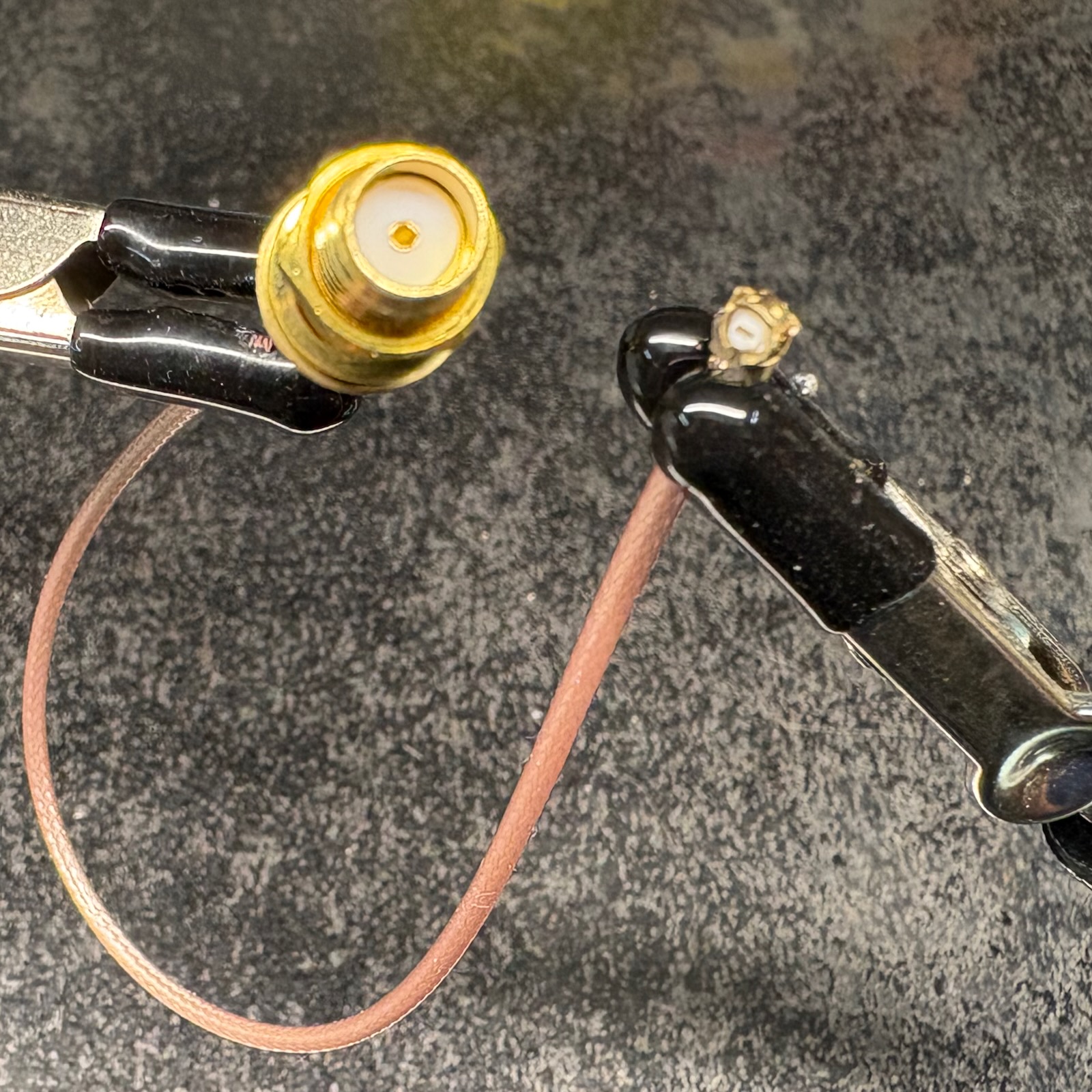
The Particle NTN antenna has a SMA connector as the antenna is typically mounted on the outside of an enclosure as a clear view of the sky is needed for proper operation.
You will typically use a U.FL to SMA bulkhead adapter. The U.FL connector connects to the CELL connector on the M636e M-SoM.
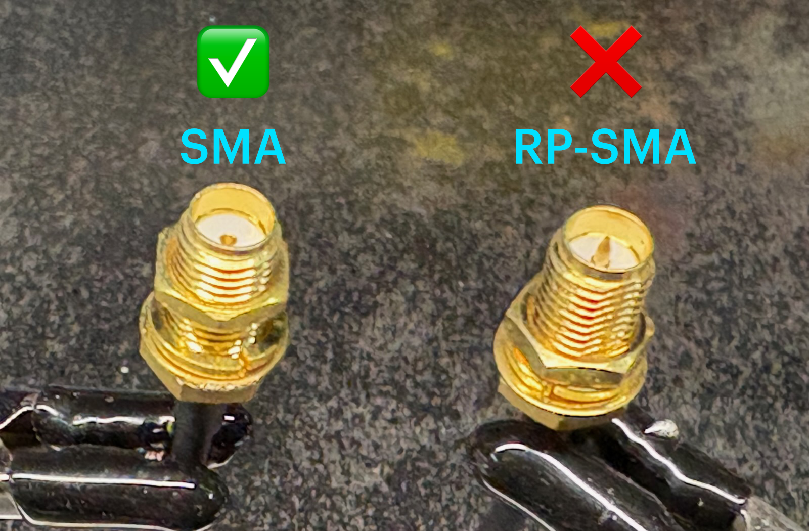
Note that there are two different styles of SMA bulkhead connectors. The PARANTCN1EA requires a standard SMA connector. Make sure you do not source a RP-SMA adapter!
General Antenna Guidance
- The antenna placement needs to follow some basic rules, as any antenna is sensitive to its environment. Mount the antenna at least 10mm from metal components or surfaces, ideally 20mm for best radiation efficiency, and try to maintain a minimum of three directions free from obstructions to be able to operate effectively.
- Needs tuning with actual product enclosure and all components.
Peripherals and GPIO
| Peripheral Type | Qty | Input(I) / Output(O) |
|---|---|---|
| Digital | 30 (max) | I/O |
| Analog (ADC) | 8 (max) | I |
| UART | 2 | I/O |
| SPI | 2 | I/O |
| I2C | 1 | I/O |
| USB | 1 | I/O |
| PWM | 11 (max) | O |
Note: All GPIOs are only rated at 3.3VDC max.
JTAG and SWD
The M-SoM has 4 pads at the bottom exposing the SWD interface of the MCU. This interface can be used to debug your code or reprogram your SoM bootloader, device OS, or the user firmware. We use 4 pogo-pins connecting to these pads during production for firmware flashing.
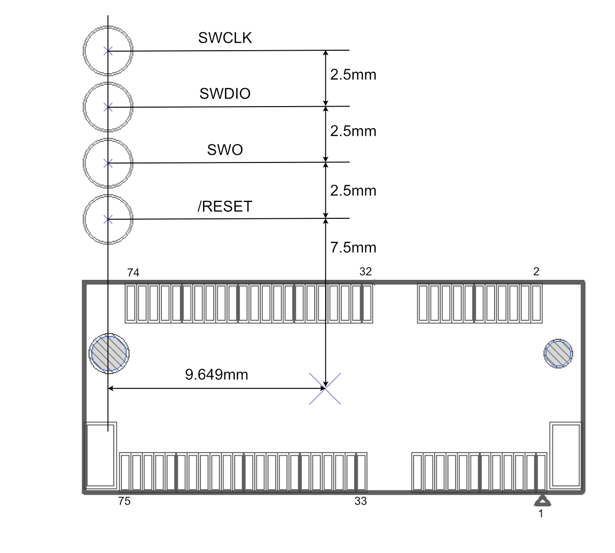
Additionally, SWD is supported on pins on the M.2 connector:
| Pin | Pin Name | Description | Interface | MCU |
|---|---|---|---|---|
| 43 | A5 / D14 | A5 Analog in, PWM, GPIO, shared with pin 53 | SWCLK | PB[3] |
| 53 | A5 / D14 | A5 Analog in, PWM, GPIO, SWCLK, shared with pin 43 | SWCLK | PB[3] |
| 55 | D27 | D27 GPIO, SWDIO (SWD_DATA), do not pull down at boot | SWDIO | PA[27] |
- SWD is on the same pins as GPIO, so by default once user firmware boots, SWD is no longer available unless SWD is enabled at compile time. This is the same as Gen 2 (STM32) but different than Gen 3 (nRF52840).
- SWO (Serial Wire Output) is not supported on the RTL8722DM.
- Pins 43 and 53 are shared
Pin information
Pinout diagram

Common SoM pins
RESERVED and SOM pins may vary across different SoM models. If you are designing for this specific module, or similar modules, you can use the indicated functions even if the pin is marked RESERVED.
The nRF52840 B-SoM has some differences from the RTL8722 M-SoM. Future modules with a different MCU may have different pin functions. An effort will be made to assign all of the listed functions for ADC, PWM, SPI, etc. from the set of common SoM pin functions in future modules, but the functions on RESERVED and SOM pins will likely vary.
Pin function by pin name
| Pin Name | Module Pin | PWM | MCU | ||||
|---|---|---|---|---|---|---|---|
| A0 / D19 | 23 | ADC_0 | ✓ | PB[4] | |||
| A1 / D18 | 33 | ADC_1 | ✓ | PB[5] | |||
| A2 / D17 | 35 | ADC_2 | PB[6] | ||||
| A3 / D16 | 37 | ADC_4 | PB[1] | ||||
| A4 / D15 | 41 | ADC_5 | PB[2] | ||||
| A5 / D14 | 43 | ADC_6 | SWCLK | ✓ | PB[3] | ||
| A5 / D14 | 53 | ADC_6 | SWCLK | ✓ | PB[3] | ||
| A6 / D29 | 45 | ADC_3 | ✓ | PB[7] | |||
| A7 / WKP | 47 | ADC_7 | PA[20] | ||||
| CELL USBD- | 46 | ||||||
| CELL USBD+ | 44 | ||||||
| CELL VBUS | 74 | ||||||
| CELL_RI | 75 | ||||||
| D0 | 22 | Wire (SDA) | PB[0] | ||||
| D1 | 20 | Wire (SCL) | PA[31] | ||||
| D2 | 42 | SPI1 (SCK) | Serial1 (RTS) | PA[14] | |||
| D3 | 40 | SPI1 (SS) | Serial1 (CTS) | PA[15] | |||
| D4 | 66 | ✓ | PB[18] | ||||
| D5 | 68 | ✓ | PB[19] | ||||
| D6 | 70 | ✓ | PB[20] | ||||
| D7 | 72 | ✓ | PB[21] | ||||
| D8 | 48 | SPI (SS) | PA[19] | ||||
| D20 | 19 | PA[1] | |||||
| D21 | 17 | PA[0] | |||||
| D22 | 62 | PA[9] | |||||
| D23 | 64 | PA[10] | |||||
| D24 | 58 | Serial2 (TX) | PA[7] | ||||
| D25 | 60 | Serial2 (RX) | PA[8] | ||||
| D26 | 59 | PA[4] | |||||
| D27 | 55 | SWDIO | PA[27] | ||||
| GNSS_TX | 18 | ||||||
| MISO / D11 | 50 | SPI (MISO) | ✓ | PA[17] | |||
| MOSI / D12 | 52 | SPI (MOSI) | ✓ | PA[16] | |||
| NC | 14 | ||||||
| RGBB | 65 | PB[22] | |||||
| RGBG | 63 | PB[23] | |||||
| RGBR | 61 | PA[30] | |||||
| RX / D10 | 38 | SPI1 (MISO) | Serial1 (RX) | ✓ | PA[13] | ||
| SCK / D13 | 54 | SPI (SCK) | PA[18] | ||||
| SIM_CLK | 71 | ||||||
| SIM_DATA | 73 | ||||||
| SIM_RST | 69 | ||||||
| SIM_VCC | 67 | ||||||
| TX / D9 | 36 | SPI1 (MOSI) | Serial1 (TX) | ✓ | PA[12] | ||
| USBDATA- | 13 | PA[25] | |||||
| USBDATA+ | 11 | PA[26] |
Pin function by M.2 pin
| Module Pin | Pin Name | PWM | MCU | ||||
|---|---|---|---|---|---|---|---|
| 11 | USBDATA+ | PA[26] | |||||
| 13 | USBDATA- | PA[25] | |||||
| 14 | NC | ||||||
| 17 | D21 | PA[0] | |||||
| 18 | GNSS_TX | ||||||
| 19 | D20 | PA[1] | |||||
| 20 | D1 | Wire (SCL) | PA[31] | ||||
| 22 | D0 | Wire (SDA) | PB[0] | ||||
| 23 | A0 / D19 | ADC_0 | ✓ | PB[4] | |||
| 33 | A1 / D18 | ADC_1 | ✓ | PB[5] | |||
| 35 | A2 / D17 | ADC_2 | PB[6] | ||||
| 36 | TX / D9 | SPI1 (MOSI) | Serial1 (TX) | ✓ | PA[12] | ||
| 37 | A3 / D16 | ADC_4 | PB[1] | ||||
| 38 | RX / D10 | SPI1 (MISO) | Serial1 (RX) | ✓ | PA[13] | ||
| 40 | D3 | SPI1 (SS) | Serial1 (CTS) | PA[15] | |||
| 41 | A4 / D15 | ADC_5 | PB[2] | ||||
| 42 | D2 | SPI1 (SCK) | Serial1 (RTS) | PA[14] | |||
| 43 | A5 / D14 | ADC_6 | SWCLK | ✓ | PB[3] | ||
| 44 | CELL USBD+ | ||||||
| 45 | A6 / D29 | ADC_3 | ✓ | PB[7] | |||
| 46 | CELL USBD- | ||||||
| 47 | A7 / WKP | ADC_7 | PA[20] | ||||
| 48 | D8 | SPI (SS) | PA[19] | ||||
| 50 | MISO / D11 | SPI (MISO) | ✓ | PA[17] | |||
| 52 | MOSI / D12 | SPI (MOSI) | ✓ | PA[16] | |||
| 53 | A5 / D14 | ADC_6 | SWCLK | ✓ | PB[3] | ||
| 54 | SCK / D13 | SPI (SCK) | PA[18] | ||||
| 55 | D27 | SWDIO | PA[27] | ||||
| 58 | D24 | Serial2 (TX) | PA[7] | ||||
| 59 | D26 | PA[4] | |||||
| 60 | D25 | Serial2 (RX) | PA[8] | ||||
| 61 | RGBR | PA[30] | |||||
| 62 | D22 | PA[9] | |||||
| 63 | RGBG | PB[23] | |||||
| 64 | D23 | PA[10] | |||||
| 65 | RGBB | PB[22] | |||||
| 66 | D4 | ✓ | PB[18] | ||||
| 67 | SIM_VCC | ||||||
| 68 | D5 | ✓ | PB[19] | ||||
| 69 | SIM_RST | ||||||
| 70 | D6 | ✓ | PB[20] | ||||
| 71 | SIM_CLK | ||||||
| 72 | D7 | ✓ | PB[21] | ||||
| 73 | SIM_DATA | ||||||
| 74 | CELL VBUS | ||||||
| 75 | CELL_RI |
GPIO (Digital I/O)
| Pin | M-SoM Pin Name | M-SoM GPIO | MCU | Special boot function |
|---|---|---|---|---|
| 17 | D21 | ✓ | PA[0] | |
| 19 | D20 | ✓ | PA[1] | |
| 20 | D1 | ✓ | PA[31] | |
| 22 | D0 | ✓ | PB[0] | |
| 23 | A0 / D19 | ✓ | PB[4] | |
| 33 | A1 / D18 | ✓ | PB[5] | |
| 35 | A2 / D17 | ✓ | PB[6] | |
| 36 | TX / D9 | ✓ | PA[12] | |
| 37 | A3 / D16 | ✓ | PB[1] | |
| 38 | RX / D10 | ✓ | PA[13] | |
| 40 | D3 | ✓ | PA[15] | |
| 41 | A4 / D15 | ✓ | PB[2] | |
| 42 | D2 | ✓ | PA[14] | |
| 43 | A5 / D14 | ✓ | PB[3] | SWCLK. 40K pull-down at boot. |
| 45 | A6 / D29 | ✓ | PB[7] | |
| 47 | A7 / WKP | ✓ | PA[20] | |
| 48 | D8 | ✓ | PA[19] | |
| 50 | MISO / D11 | ✓ | PA[17] | |
| 52 | MOSI / D12 | ✓ | PA[16] | |
| 53 | A5 / D14 | ✓ | PB[3] | SWCLK. 40K pull-down at boot. |
| 54 | SCK / D13 | ✓ | PA[18] | |
| 55 | D27 | ✓ | PA[27] | SWDIO. 40K pull-up at boot. Low at boot triggers MCU test mode. |
| 58 | D24 | ✓ | PA[7] | Low at boot triggers ISP flash download |
| 59 | D26 | ✓ | PA[4] | |
| 60 | D25 | ✓ | PA[8] | Goes high at boot |
| 62 | D22 | ✓ | PA[9] | |
| 64 | D23 | ✓ | PA[10] | |
| 66 | D4 | ✓ | PB[18] | |
| 68 | D5 | ✓ | PB[19] | |
| 70 | D6 | ✓ | PB[20] | |
| 72 | D7 | ✓ | PB[21] |
- All GPIO are 3.3V only and are not 5V tolerant
- The drive strength is 4 mA per pin in normal drive and 12 mA per pin in high drive mode on the M-SoM.
- There is a maximum of 200 mA across all pins. The total maximum could be further limited by your 3.3V regulator.
- Drive strength selection using pinSetDriveStrength is only available in Device OS 5.5.0 and later on the M-SoM.
Certain GPIO will change state at boot, or cause the MCU to enter a special mode. See the boot mode pins section, below, for more information.
ADC (Analog to Digital Converter)
| Pin | Pin Name | Description | Interface | MCU |
|---|---|---|---|---|
| 23 | A0 / D19 | A0 Analog in, GPIO, PWM | ADC_0 | PB[4] |
| 33 | A1 / D18 | A1 Analog in, GPIO, PWM | ADC_1 | PB[5] |
| 35 | A2 / D17 | A2 Analog in, GPIO | ADC_2 | PB[6] |
| 37 | A3 / D16 | A3 Analog in, PDM CLK, GPIO | ADC_4 | PB[1] |
| 41 | A4 / D15 | A4 Analog in, PDM DAT, GPIO | ADC_5 | PB[2] |
| 43 | A5 / D14 | A5 Analog in, PWM, GPIO, shared with pin 53 | ADC_6 | PB[3] |
| 45 | A6 / D29 | A6 Analog in, GPIO, PWM, M.2 eval PMIC INT | ADC_3 | PB[7] |
| 47 | A7 / WKP | A7 Analog In, WKP, GPIO D28 | ADC_7 | PA[20] |
| 53 | A5 / D14 | A5 Analog in, PWM, GPIO, SWCLK, shared with pin 43 | ADC_6 | PB[3] |
- ADC inputs are single-ended and limited to 0 to 3.3V
- Resolution is 12 bits
- SoM pin 43 (A5) on the M-SoM is shared with SoM pin 53 (SWD_CLK). You cannot use A5 and SWD at the same time. If you implement SWD on your base board, driving pin A6 will prevent SWD from functioning. The SWD_CLK will be driven at boot by the MCU.
The ADCs on the M-SoM (RTL872x) have a lower impedance than other Particle device MCUs (nRF52, STM32F2xx). They require a stronger drive and this may cause issues when used with a voltage divider. This is particularly true for A7, which has an even lower impedance than other ADC inputs.
For signals that change slowly, such as NTC thermocouple resistance, you can add a 2.2 uF capacitor to the signal. For rapidly changing signals, a voltage follower IC can be used.
UART serial
| Pin | Pin Name | Description | Interface | MCU |
|---|---|---|---|---|
| 36 | TX / D9 | Serial TX, PWM, GPIO, SPI1 MOSI, I2S MCLK | Serial1 (TX) | PA[12] |
| 38 | RX / D10 | Serial RX, PWM, GPIO, SPI1 MISO | Serial1 (RX) | PA[13] |
| 40 | D3 | D3 GPIO, Serial1 CTS flow control (optional), SPI1 SS | Serial1 (CTS) | PA[15] |
| 42 | D2 | D2 GPIO, Serial RTS flow control (optional), SPI1 SCK | Serial1 (RTS) | PA[14] |
| 58 | D24 | D24 GPIO, Serial2 TX, do not pull down at boot | Serial2 (TX) | PA[7] |
| 60 | D25 | GPIO25, Serial2 RX | Serial2 (RX) | PA[8] |
- The UART pins are 3.3V and must not be connected directly to a RS-232C port or to a 5V TTL serial port
- Hardware flow control is optional; if not used then the RTS and CTS pins can be used as regular GPIO
- Serial1 uses the RTL872x UART_LOG peripheral
- Serial2 uses the RTL872x HS_UART0 peripheral
- Supported baud rates: 110, 300, 600, 1200, 2400, 4800, 9600, 14400, 19200, 28800, 38400, 57600, 76800, 115200, 128000, 153600, 230400, 380400, 460800, 500000, 921600, 1000000, 1382400, 1444400, 1500000, 1843200, 2000000, 2100000, 2764800, 3000000, 3250000, 3692300, 3750000, 4000000, 6000000
SPI
| Pin | Pin Name | Description | Interface | MCU |
|---|---|---|---|---|
| 36 | TX / D9 | Serial TX, PWM, GPIO, SPI1 MOSI, I2S MCLK | SPI1 (MOSI) | PA[12] |
| 38 | RX / D10 | Serial RX, PWM, GPIO, SPI1 MISO | SPI1 (MISO) | PA[13] |
| 40 | D3 | D3 GPIO, Serial1 CTS flow control (optional), SPI1 SS | SPI1 (SS) | PA[15] |
| 42 | D2 | D2 GPIO, Serial RTS flow control (optional), SPI1 SCK | SPI1 (SCK) | PA[14] |
| 48 | D8 | D8 GPIO, SPI SS | SPI (SS) | PA[19] |
| 50 | MISO / D11 | D11 GPIO, PWM, SPI MISO | SPI (MISO) | PA[17] |
| 52 | MOSI / D12 | D12 GPIO, PWM, SPI MOSI | SPI (MOSI) | PA[16] |
| 54 | SCK / D13 | D13 GPIO, SPI SCK | SPI (SCK) | PA[18] |
- The SPI port is 3.3V and must not be connected directly to devices that drive MISO at 5V
- If not using a SPI port, its pins can be used as GPIO
- Any pins can be used as the SPI chip select
- Multiple devices can generally share a single SPI port
- SPI uses the RTL872x SPI0 peripheral (50 MHz maximum speed)
- SPI1 uses the RTL872x SPI1 peripheral (25 MHz maximum speed)
- Note: The P2/Photon 2 maximum speeds for SPI and SPI1 are reversed from the M-SoM
Even though the B-SoM and M-SoM both have two SPI interfaces, note that the M-SoM SPI1 is on different pins.
| Pin | B-SoM Pin Name | B-SoM SPI | M-SoM Pin Name | M-SoM SPI |
|---|---|---|---|---|
| 36 | TX / D9 | TX / D9 | SPI1 (MOSI) | |
| 38 | RX / D10 | RX / D10 | SPI1 (MISO) | |
| 40 | D3 | SPI1 (MOSI) | D3 | SPI1 (SS) |
| 42 | D2 | SPI1 (SCK) | D2 | SPI1 (SCK) |
| 48 | D8 | SPI (SS) | D8 | SPI (SS) |
| 50 | MISO / D11 | SPI (MISO) | MISO / D11 | SPI (MISO) |
| 52 | MOSI / D12 | SPI (MOSI) | MOSI / D12 | SPI (MOSI) |
| 54 | SCK / D13 | SPI (SCK) | SCK / D13 | SPI (SCK) |
| 66 | D4 | SPI1 (MISO) | D4 |
I2C
| Pin | Pin Name | Description | Interface | MCU |
|---|---|---|---|---|
| 20 | D1 | D1 GPIO, I2C SCL | Wire (SCL) | PA[31] |
| 22 | D0 | D0 GPIO, I2C SDA | Wire (SDA) | PB[0] |
- The I2C port is 3.3V and must not be connected directly a 5V I2C bus
- Maximum bus speed is 400 kHz
- External pull-up resistors are required for I2C
PWM
| Pin | Pin Name | Description | MCU |
|---|---|---|---|
| 23 | A0 / D19 | A0 Analog in, GPIO, PWM | PB[4] |
| 33 | A1 / D18 | A1 Analog in, GPIO, PWM | PB[5] |
| 36 | TX / D9 | Serial TX, PWM, GPIO, SPI1 MOSI, I2S MCLK | PA[12] |
| 38 | RX / D10 | Serial RX, PWM, GPIO, SPI1 MISO | PA[13] |
| 43 | A5 / D14 | A5 Analog in, PWM, GPIO, shared with pin 53 | PB[3] |
| 45 | A6 / D29 | A6 Analog in, GPIO, PWM, M.2 eval PMIC INT | PB[7] |
| 50 | MISO / D11 | D11 GPIO, PWM, SPI MISO | PA[17] |
| 52 | MOSI / D12 | D12 GPIO, PWM, SPI MOSI | PA[16] |
| 53 | A5 / D14 | A5 Analog in, PWM, GPIO, SWCLK, shared with pin 43 | PB[3] |
| 66 | D4 | D4 GPIO, PWM | PB[18] |
| 68 | D5 | D5 GPIO, PWM, I2S TX | PB[19] |
| 70 | D6 | D6 GPIO, PWM, I2S CLK | PB[20] |
| 72 | D7 | D7 GPIO, PWM, I2S WS | PB[21] |
- All available PWM pins on the M-SoM share a single timer. This means that they must all share a single frequency, but can have different duty cycles.
PDM
Pulse density modulation digital microphones can be used with the Microphone_PDM library and the M-SoM, but only on specific pins:
| Pin | Pin Name | Description | MCU |
|---|---|---|---|
| 37 | A3 / D16 | A3 Analog in, PDM CLK, GPIO | PB[1] |
| 41 | A4 / D15 | A4 Analog in, PDM DAT, GPIO | PB[2] |
USB
The M-SoM supports a USB interface for programming the device and for USB serial (CDC) communications. The module itself does not contain a USB connector; you typically add a micro USB or USB C connector on your base board. It is optional but recommended.
| Pin | Pin Name | Description | MCU |
|---|---|---|---|
| 11 | USBDATA+ | USB Data+ | PA[26] |
| 13 | USBDATA- | USB Data- | PA[25] |
| 44 | CELL USBD+ | Cellular Modem USB Data+ | |
| 46 | CELL USBD- | Cellular Modem USB Data- |
- The CELL USB connector does not need to be populated on your board. It is used for reprogramming the cellular modem firmware, which is rarely done as it often requires recertification of the device.
RGB LED
The M-SoM supports an external common anode RGB LED.
One common LED that meets the requirements is the Cree CLMVC-FKA-CL1D1L71BB7C3C3 which is inexpensive and easily procured. You need to add three current limiting resistors. With this LED, we typically use 1K ohm current limiting resistors. These are much larger than necessary. They make the LED less blinding but still provide sufficient current to light the LEDs. If you want maximum brightness you should use the calculated values - 33 ohm on red, and 66 ohm on green and blue.
A detailed explanation of different color codes of the RGB system LED can be found here.
The use of the RGB LED is optional, however it is highly recommended as troubleshooting the device without the LED is very difficult.
| Pin | Pin Name | Description | MCU |
|---|---|---|---|
| 61 | RGBR | RGB LED Red | PA[30] |
| 63 | RGBG | RGB LED Green | PB[23] |
| 65 | RGBB | RGB LED Blue | PB[22] |
- On the M-SoM, Pin RGBR (PA[30]) has a 10K hardware pull-up in the module because it's a trap pin that controls the behavior of the internal 1.1V regulator. This does not affect the RGB LED but could affect your design if you are repurposing this pin as GPIO. You must not hold this pin low at boot.
Boot mode pins
These pins have a special function at boot. Beware when using these pins as input as they can trigger special modes in the MCU.
| Pin | Pin Name | Description | MCU |
|---|---|---|---|
| 43 | A5 / D14 | SWCLK. 40K pull-down at boot. | PB[3] |
| 53 | A5 / D14 | SWCLK. 40K pull-down at boot. | PB[3] |
| 55 | D27 | SWDIO. 40K pull-up at boot. Low at boot triggers MCU test mode. | PA[27] |
| 58 | D24 | Low at boot triggers ISP flash download | PA[7] |
| 60 | D25 | Goes high at boot | PA[8] |
| 61 | RGBR | Low at boot triggers trap mode | PA[30] |
BLE (Bluetooth LE)
If you wish to use Wi-Fi on the M-SoM you will need to provide a way to configure it. Wi-Fi setup works the same as the P2, Photon 2, and Argon, and uses BLE. See Wi-Fi setup options for more information.
BLE 5.3 BLE Central Mode and BLE Peripheral Mode are supported.
Full-speed BLE modes such as A2DP used for BLE audio are not supported.
Wi-Fi and BLE share the same antenna so you do not need to include a separate antenna to use both.
Sleep
The M-SoM can wake from STOP or ULTRA_LOW_POWER sleep mode on any GPIO, RISING, FALLING, or CHANGE.
The M-SoM can only wake from HIBERNATE sleep mode on certain pins, RISING, FALLING, or CHANGE.
The M-SoM preserves the state of outputs during STOP or ULTRA_LOW_POWER sleep mode. In HIBERNATE, outputs are high-impedance.
| Pin | Pin Name | Description | Interface | MCU |
|---|---|---|---|---|
| 36 | TX / D9 | Serial TX, PWM, GPIO, SPI1 MOSI, I2S MCLK | Pin can wake from HIBERNATE sleep | PA[12] |
| 38 | RX / D10 | Serial RX, PWM, GPIO, SPI1 MISO | Pin can wake from HIBERNATE sleep | PA[13] |
| 40 | D3 | D3 GPIO, Serial1 CTS flow control (optional), SPI1 SS | Pin can wake from HIBERNATE sleep | PA[15] |
| 42 | D2 | D2 GPIO, Serial RTS flow control (optional), SPI1 SCK | Pin can wake from HIBERNATE sleep | PA[14] |
| 47 | A7 / WKP | A7 Analog In, WKP, GPIO D28 | Pin can wake from HIBERNATE sleep | PA[20] |
| 48 | D8 | D8 GPIO, SPI SS | Pin can wake from HIBERNATE sleep | PA[19] |
| 50 | MISO / D11 | D11 GPIO, PWM, SPI MISO | Pin can wake from HIBERNATE sleep | PA[17] |
| 52 | MOSI / D12 | D12 GPIO, PWM, SPI MOSI | Pin can wake from HIBERNATE sleep | PA[16] |
| 54 | SCK / D13 | D13 GPIO, SPI SCK | Pin can wake from HIBERNATE sleep | PA[18] |
Most pins can use INPUT_PULLUP or INPUT_PULLDOWN in sleep modes. The exception is HIBERNATE sleep mode where pin D21 can only use an external hardware pull-up or pull down. It also cannot be used to wake from hibernate sleep mode.
| Pin | Pin Name | Description | Interface | MCU |
|---|---|---|---|---|
| 17 | D21 | D21 GPIO, I2S RX | No internal pull up or pull down in HIBERNATE sleep mode. | PA[0] |
SETUP and RESET button
It is highly recommended that you add MODE (SETUP) and RESET buttons to your base board using momentary switches that connect to GND. These are necessary to change the operating mode of the device, for example to enter listening or DFU mode.
| Pin | Pin Name | Description | MCU |
|---|---|---|---|
| 32 | MODE | MODE button. Pin number constant is BTN. External pull-up required! | PA[11] |
| 34 | RST | Hardware reset, active low. External pull-up required. | CHIP_EN |
The MODE button does not have a hardware pull-up on it, so you must add an external pull-up (2.2K to 10K) to 3V3, or connect it to 3V3 if not using a button.
The RST pin does have an internal weak pull-up, but you may want to add external pull-up on that as well, especially if you use an off-board reset button connected by long wires.
Supervisory reset
In many cases, it may be desirable to include a supervisory reset IC in your design. The design below is from the Photon 2 and uses the small and inexpensive Richtec RT9818C. This chip will hold the MCU in reset until there is sufficient voltage to successfully boot. This can be helpful if your power supply cannot guarantee a sufficient slew rate.
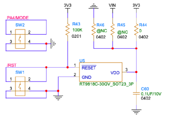
Of note in this design, the VDD pin of the RT9818C is connected to 3V3. The design is configurable by moving a zero-ohm resistor to disable supervisory reset (by connecting to GND) or to use VIN. Note that the RT9818C has a maximum input voltage of 6V which is compatible with the Photon 2. Keep this in mind if using VIN on designs that have larger VIN voltages.
Of course you can simply wire VDD to 3V3 instead of including the configurable resistors.
PMIC Notes
When using the M-SoM with a bq24195 PMIC, note the following:
By default, the bq24195 sets the input current limit, which affects powering by VIN and VUSB, to 100 mA. This affects the VSYS output of the PMIC, which powers both the cellular modem and 3V3 supply, and is not enough to power the M-SoM in normal operation.
If your device has the default firmware (Tinker), it will attempt to connect to the cloud, brown out due to insufficient current, then the device will reset. This may result in what appears to be the status LED blinking white, but is actually rolling reboot caused by brownout.
A factory new M-SoM does not enable the PMIC setup. To enable the use of the bq21415, you must enable the system power feature PMIC_DETECTION in your code. This defaults to off because the M-SoM can be used without a PMIC, or with a different PMIC, and also requires I2C on D0/D1, and some base boards may use those pins as GPIO.
Because the input current limit does not affect the battery input (Li+), for troubleshooting purposes it can be helpful to attach a battery to help rule out input current limit issues. It's also possible to supply 3.7V via a bench power supply to the battery input, instead of VIN.
The input current limit can result in a situation where you can't bring up a M-SoM because it browns out continuously, but also cannot flash code to it to stop if from browning out. There are two general solutions:
- Attach a battery or supply by Li+ when bringing up a board.
- Use SWD/JTAG and reset halt the MCU. This will prevent it from connecting to the cloud, so you can flash Device OS and firmware to it by SWD.
The input current limit is actually controlled by three factors:
- The power source max current setting in the PMIC. The default is 900 mA. It can be set to 100, 150, 500, 900, 1200, 1500, 2000, or 3000 mA.
- It is also limited by the hardware ILIM resistor. On Particle devices with a built-in PMIC, this is set to 1590 mA, but if you are implementing your own PMIC hardware, you can adjust this higher.
- When connected by USB, it will use DPDM, current negotiation via the USB DP (D+) and DM (D-) lines.
Note that some 2A tablet chargers and multi-port USB power supplies supply 2A but do not implement DPDM; these will be treated as if VIN was used, and you must set the power source current, otherwise the input current will be limited to 900 mA, which is not enough to power a 2G/3G cellular modem without an attached battery.
Cellular modem USB pins
The cellular modem USB pins are optional on custom base boards. These pins are used for low-level diagnostics and reprogramming the cellular modem firmware.
Note, however, the Particle has never done a cellular modem firmware upgrade in the field because doing so generally requires recertification, and is there is a high likelihood that the upgrade will fail, rendering the modem unusable.
Cellular modem could be reprogrammed by removing the SoM from your board and putting it in the M.2 SoM breakout board, which has the cellular modem USB connector.
| # | Pin | Common | Function | nRF52 | Description |
|---|---|---|---|---|---|
| 44 | Quectel USB D+ | SOM0 | IO | Data+ pin of the cellular modem USB port. | |
| 46 | Quectel USB D- | SOM1 | IO | Data- pin of the cellular modem USB port. | |
| 74 | Quectel VBUS | SOM23 | IO | USB detect pin for cellular modem. 5V on this pin enables the Quectel USB interface. | |
| 75 | Quectel RI | SOM94 | IO | Ring indicator |
SIM Pins
- The SIM pins should be left unconnected
- You cannot use these pins for an external SIM card, despite their names
| Pin | Pin Name | Description |
|---|---|---|
| 69 | SIM_RST | Leave unconnected, 1.8V/3V SIM Reset Output from cellular modem. |
| 71 | SIM_CLK | Leave unconnected, 1.8V/3V SIM Clock Output from cellular modem. |
| 73 | SIM_DATA | Leave unconnected, 1.8V/3V SIM Data I/O of cellular modem with internal 4.7 k pull-up. |
Technical specification
I/O Characteristics
| Parameter | Symbol | Min | Typ | Peak | Unit |
|---|---|---|---|---|---|
| Input-High Voltage | VIH | 2.0 | V | ||
| Input-Low Voltage | VIL | 0.8 | V | ||
| Output drive strength (normal drive) | 4 | mA | |||
| Output drive strength (high drive) | 12 | mA | |||
| Total output drive (all pins) | 200 | mA |
Power consumption (M524)
| Parameter | Symbol | Min | Typ | Peak | Unit |
|---|---|---|---|---|---|
| Operating current (uC on, peripherals and radio disabled) | Iidle | 26.4 | 26.6 | 26.9 | mA |
| Operating current (uC on, BLE advertising) | Ible_adv | 62.9 | 66.1 | 84.2 | mA |
| Operating current (uC on, BLE connected but idle) | Ible_conn_idle | 62.4 | 66.7 | 74 | mA |
| Operating current (uC on, BLE scanning) | Ible_scan | 50.5 | 57.2 | 87.7 | mA |
| Operating current (uC on, cellular on but not connected) | Icell_idle | 36.7 | 44.4 | 907 | mA |
| Operating current (uC on, cellular connecting to cloud) | Icell_conn_cloud | 40.2 | 97.4 | 840 | mA |
| Operating current (uC on, cellular connected but idle) | Icell_cloud_idle | 37 | 43.1 | 132 | mA |
| Operating current (uC on, cellular connected and transmitting) | Icell_cloud_tx | 39.9 | 164 | 851 | mA |
| Operating current (uC on, Wi-Fi on but not connected) | Iwifi_idle | 26.1 | 26.3 | 26.6 | mA |
| Operating current (uC on, Wi-Fi connecting to access point) | Iwifi_conn_ap | 44.3 | 67.3 | 298 | mA |
| Operating current (uC on, Wi-Fi connecting to cloud) | Iwifi_conn_cloud | 61 | 68.2 | 357 | mA |
| Operating current (uC on, Wi-Fi connected but idle) | Iwifi_cloud_idle | 61.9 | 64.1 | 68.4 | mA |
| Operating current (uC on, Wi-Fi connected and transmitting) | Iwifi_cloud_tx | 60.1 | 64.8 | 309 | mA |
| STOP mode sleep, GPIO wake-up | Istop_gpio | 419 | 421 | 425 | uA |
| STOP mode sleep, RTC wake-up | Istop_intrtc | 412 | 415 | 418 | uA |
| ULP mode sleep, GPIO wake-up | Iulp_gpio | 419 | 421 | 425 | uA |
| ULP mode sleep, RTC wake-up | Iulp_intrtc | 412 | 415 | 418 | uA |
| HIBERNATE mode sleep, GPIO wake-up | Ihib_gpio | 23.9 | 26.1 | 28.6 | uA |
| HIBERNATE mode sleep, RTC wake-up | Ihib_intrtc | 24.5 | 26.5 | 28.1 | uA |
1The min, and particularly peak, values may consist of very short transients. The typical (typ) values are the best indicator of overall power consumption over time. The peak values indicate the absolute minimum capacity of the power supply necessary, not overall consumption.
Current measurements taken at 3.6V via the battery input. For more information about measuring power usage, see power measurement.
Power consumption (M404)
| Parameter | Symbol | Min | Typ | Peak | Unit |
|---|---|---|---|---|---|
| Operating current (uC on, peripherals and radio disabled) | Iidle | 27.7 | 27.9 | 28.1 | mA |
| Operating current (uC on, BLE advertising) | Ible_adv | 65.5 | 69.5 | 85.9 | mA |
| Operating current (uC on, BLE connected but idle) | Ible_conn_idle | 65.5 | 70.1 | 77 | mA |
| Operating current (uC on, BLE scanning) | Ible_scan | 52.6 | 60.5 | 91.1 | mA |
| Operating current (uC on, cellular connected and transmitting) | Icell_cloud_tx | 36.2 | 159 | 816 | mA |
| Operating current (uC on, cellular on but not connected using LTE Cat M1) | Icell_idle_catm1 | 41.5 | 46.7 | 217 | mA |
| Operating current (uC on, cellular connecting to tower using LTE Cat M1) | Icell_conn_twr_catm1 | 39.8 | 43.9 | 131 | mA |
| Operating current (uC on, cellular connecting to cloud using LTE Cat M1) | Icell_conn_cloud_catm1 | 39.7 | 83.5 | 181 | mA |
| Operating current (uC on, cellular connected but idle using LTE Cat M1) | Icell_cloud_idle_catm1 | 41.8 | 44.5 | 155 | mA |
| Operating current (uC on, cellular connected and transmitting using LTE Cat M1) | Icell_cloud_tx_catm1 | 40.1 | 83.6 | 177 | mA |
| Operating current (uC on, cellular on but not connected using 2G) | Icell_idle_2g | 38.9 | 44.7 | 1700 | mA |
| Operating current (uC on, cellular connecting to tower using 2G) | Icell_conn_twr_2g | 36.9 | 128 | 1700 | mA |
| Operating current (uC on, cellular connecting to cloud using 2G) | Icell_conn_cloud_2g | 35.9 | 98.3 | 1740 | mA |
| Operating current (uC on, cellular connected but idle using 2G) | Icell_cloud_idle_2g | 35.8 | 40.3 | 114 | mA |
| Operating current (uC on, cellular connected and transmitting using 2G) | Icell_cloud_tx_2g | 32 | 152 | 1720 | mA |
| Operating current (uC on, Wi-Fi on but not connected) | Iwifi_idle | 27.3 | 30.4 | 101 | mA |
| Operating current (uC on, Wi-Fi connecting to access point) | Iwifi_conn_ap | 25.4 | 68.9 | 353 | mA |
| Operating current (uC on, Wi-Fi connecting to cloud) | Iwifi_conn_cloud | 59.8 | 109 | 469 | mA |
| Operating current (uC on, Wi-Fi connected but idle) | Iwifi_cloud_idle | 61.6 | 64.5 | 184 | mA |
| Operating current (uC on, Wi-Fi connected and transmitting) | Iwifi_cloud_tx | 60.7 | 64.9 | 349 | mA |
| STOP mode sleep, GPIO wake-up | Istop_gpio | 542 | 547 | 551 | uA |
| STOP mode sleep, RTC wake-up | Istop_intrtc | 512 | 515 | 518 | uA |
| ULP mode sleep, GPIO wake-up | Iulp_gpio | 542 | 547 | 551 | uA |
| ULP mode sleep, RTC wake-up | Iulp_intrtc | 512 | 515 | 518 | uA |
| HIBERNATE mode sleep, GPIO wake-up | Ihib_gpio | 41.9 | 44 | 45.8 | uA |
| HIBERNATE mode sleep, RTC wake-up | Ihib_intrtc | 41.1 | 43.4 | 45.3 | uA |
1The min, and particularly peak, values may consist of very short transients. The typical (typ) values are the best indicator of overall power consumption over time. The peak values indicate the absolute minimum capacity of the power supply necessary, not overall consumption.
Current measurements taken at 3.6V via the battery input. For more information about measuring power usage, see power measurement.
Power consumption (M635)
To be determined at a later date. When operated on LTE Cat M1 or 2G, should be similar to M404.
Radio specifications
Realtek RTL872x for Wi-Fi 2.4 GHz
| Feature | Description | Minimum | Typical | Maximum | Unit |
|---|---|---|---|---|---|
| Frequency Range | Center channel | 2412 | - | 2484 | MHz |
| Output power | 1 Mbps CCK | - | 20 | 21 | dBM |
| 11 Mbps CCK | - | 18 | 21 | dBM | |
| BPSK rate 1/2, 6Mbps OFDM | - | 20 | 21 | dBM | |
| 64QAM rate 3/4, 54Mbps OFDM | - | 17 | 18 | dBM | |
| HT20-MCS 0, BPSK rate 1/2 | - | 19 | 20 | dBM | |
| HT20-MCS 7, 64QAM rate 5/6 | - | 16 | 17 | dBM | |
| HT40-MCS 0, BPSK rate 1/2 | - | 19 | 20 | dBM | |
| HT40-MCS 7, 64QAM rate 5/6 | - | 16 | 17 | dBM | |
| Tx EVM | BPSK rate 1/2, 6Mbps OFDM | - | - | -5 | dB |
| 64QAM rate 3/4, 54Mbps OFDM | - | - | -25 | dB | |
| HT20-MCS 0, BPSK rate 1/2 | - | - | -5 | dB | |
| HT20-MCS 7, 64QAM rate 5/6 | - | - | -28 | dB | |
| HT40-MCS 0, BPSK rate 1/2 | - | - | -5 | dB | |
| HT40-MCS 7, 64QAM rate 5/6 | - | - | -28 | dB | |
| Output power variation | -1.5 | - | 1.5 | dBm | |
| Carrier suppression | - | - | -30 | dBm |
Realtek RTL872x for Wi-Fi 5 GHz
| Feature | Description | Minimum | Typical | Maximum | Unit |
|---|---|---|---|---|---|
| Frequency Range | Center channel | 5180 | - | 5825 | MHz |
| Output power | BPSK rate 1/2, 6Mbps OFDM | - | 19 | 19 | dBM |
| 64QAM rate 3/4, 54Mbps OFDM | - | 14 | 15 | dBM | |
| HT20-MCS 0, BPSK rate 1/2 | - | 17 | 18 | dBM | |
| HT20-MCS 7, 64QAM rate 5/6 | - | 13 | 14 | dBM | |
| HT40-MCS 0, BPSK rate 1/2 | - | 17 | 18 | dBM | |
| HT40-MCS 7, 64QAM rate 5/6 | - | 13 | 14 | dBM | |
| Tx EVM | BPSK rate 1/2, 6Mbps OFDM | - | - | -5 | dB |
| 64QAM rate 3/4, 54Mbps OFDM | - | - | -25 | dB | |
| HT20-MCS 0, BPSK rate 1/2 | - | - | -5 | dB | |
| HT20-MCS 7, 64QAM rate 5/6 | - | - | -28 | dB | |
| HT40-MCS 0, BPSK rate 1/2 | - | - | -5 | dB | |
| HT40-MCS 7, 64QAM rate 5/6 | - | - | -28 | dB | |
| Output power variation | -1.5 | - | 1.5 | dBm | |
| Carrier suppression | - | - | -30 | dBm |
Realtek RTL872x for BLE
| Feature | Description | Minimum | Typical | Maximum | Unit |
|---|---|---|---|---|---|
| Frequency Range | 2402 | - | 2480 | MHz | |
| Tx Output power | -10 | 4.5 | dBM |
Cellular characteristics for BG95-M5 (M404)
| Parameter | Value | |
|---|---|---|
| Protocol stack | 3GPP Release 14 | |
| RAT | LTE Cat M1 | |
| LTE FDD Bands | Band 12 (700 MHz) | |
| Band 13 (700 MHz) | ||
| Band 28 (700 MHz) | ||
| Band 20 (800 MHz) | ||
| Band 5 (850 MHz) | ||
| Band 26 (850 MHz) | ||
| Band 8 (900 MHz) | ||
| Band 4 (1700 MHz) | ||
| Band 3 (1800 MHz) | ||
| Band 2 (1900 MHz) | ||
| Band 25 (1900 MHz) | ||
| Band 1 (2100 MHz) | ||
| Band 66 (2100 MHz) | ||
| GSM Bands | GSM850 (850 MHz) | |
| EGSM900 (900 MHz) | ||
| DCS1800 (1800 MHz) | ||
| PCS1900 (1900 MHz) | ||
| Power class | Class 4 (33dBm ± 2dB) for GSM850 | |
| Class 4 (33dBm ± 2dB) for EGSM900 | ||
| Class 1 (30dBm ± 2dB) for DCS1800 | ||
| Class 1 (30dBm ± 2dB) for PCS1900 | ||
| Class E2 (27dBm ± 3dB) for GSM850 8-PSK | ||
| Class E2 (27dBm ± 3dB) for EGSM900 8-PSK | ||
| Class E2 (26dBm ± 3dB) for DCS1800 8-PSK | ||
| Class E2 (26dBm ± 3dB) for PCS1900 8-PSK | ||
| Class 3 (23dBm ± 2dB) for LTE FDD bands |
Cellular characteristics for EG91-EX (M524)
| Parameter | Value |
|---|---|
| Protocol stack | 3GPP Release 13 |
| RAT | LTE Cat 1 |
| LTE FDD Bands | Band 28A (700 MHz) |
| Band 20 (800 MHz) | |
| Band 8 (900 MHz) | |
| Band 3 (1800 MHz) | |
| Band 1 (2100 MHz) | |
| Band 7 (2600 MHz) | |
| WCDMA Bands | Band 8 (900 MHz) |
| Band 1 (2100) | |
| GSM Bands | EGSM900 (900 MHz) |
| DCS1800 (1800 MHz) | |
| Power class | Class 4 (33dBm ± 2dB) for EGSM900 |
| Class 1 (30dBm ± 2dB) for DCS1800 | |
| Class E2 (27dBm ± 3dB) for EGSM900 8-PSK | |
| Class E2 (26dBm ± 3dB) for DCS1800 8-PSK | |
| Class 3 (24dBm ± 3dB) for WCDMA bands | |
| Class 3 (23dBm ± 2dB) for LTE FDD bands |
Cellular characteristics for BG95-S5 (M635e)
| Parameter | Value | |
|---|---|---|
| Protocol stack | 3GPP Release 14 | |
| RAT | LTE Cat M1 | |
| IoT-NTN | ||
| EGPRS | ||
| LTE FDD Bands | Band 71 (600 MHz) | |
| Band 12 (700 MHz) | ||
| Band 13 (700 MHz) | ||
| Band 28 (700 MHz) | ||
| Band 85 (700 MHz) | ||
| Band 20 (800 MHz) | ||
| Band 5 (850 MHz) | ||
| Band 18 (850 MHz) | ||
| Band 19 (850 MHz) | ||
| Band 26 (850 MHz) | ||
| Band 8 (900 MHz) | ||
| Band 4 (1700 MHz) | ||
| Band 3 (1800 MHz) | ||
| Band 2 (1900 MHz) | ||
| Band 25 (1900 MHz) | ||
| Band 1 (2100 MHz) | ||
| Band 66 (2100 MHz) | ||
| GSM Bands | GSM850 (850 MHz) | |
| EGSM900 (900 MHz) | ||
| DCS1800 (1800 MHz) | ||
| PCS1900 (1900 MHz) | ||
| IoT-NTN Bands | B23/B256 (S-Band) | |
| B244 (L-Band) | ||
| Power class | Class 4 (33dBm ± 2dB) for GSM850 | |
| Class 4 (33dBm ± 2dB) for EGSM900 | ||
| Class 1 (30dBm ± 2dB) for DCS1800 | ||
| Class 1 (30dBm ± 2dB) for PCS1900 | ||
| Class E2 (27dBm ± 3dB) for GSM850 8-PSK | ||
| Class E2 (27dBm ± 3dB) for EGSM900 8-PSK | ||
| Class E2 (26dBm ± 3dB) for DCS1800 8-PSK | ||
| Class E2 (26dBm ± 3dB) for PCS1900 8-PSK | ||
| Class 3 (23dBm ± 2dB) for LTE FDD bands | ||
| Class 3 (23 dBm ± 2.7 dB) for IoT-NTN bands |
Mechanical specifications
Mechanical drawing
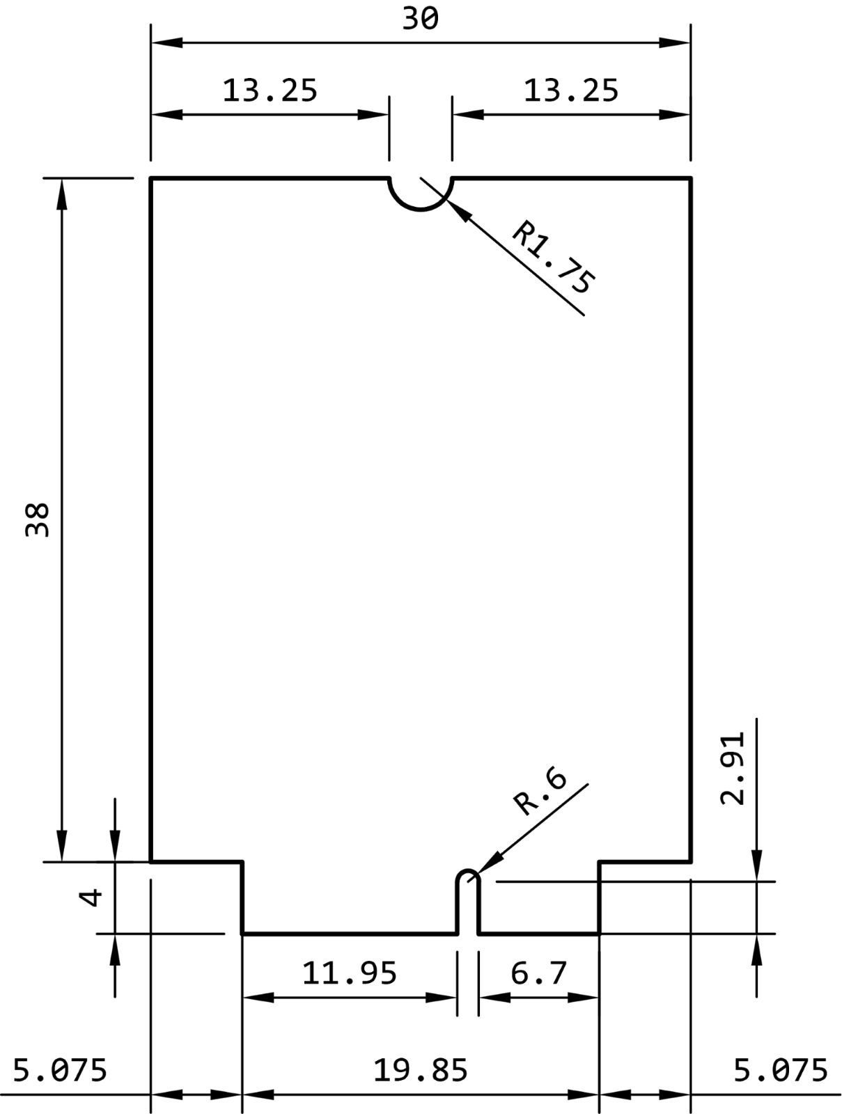
Dimensions are in millimeters.
Mating connector and land pattern
The mating connector is a an M.2 (NGFF) type 4. Note that there are several different key configurations for the M.2, and type 4 is different than is commonly used on SSDs.
One compatible connector is the TE 2199230-4. It is widely available including at suppliers such as DigiKey.
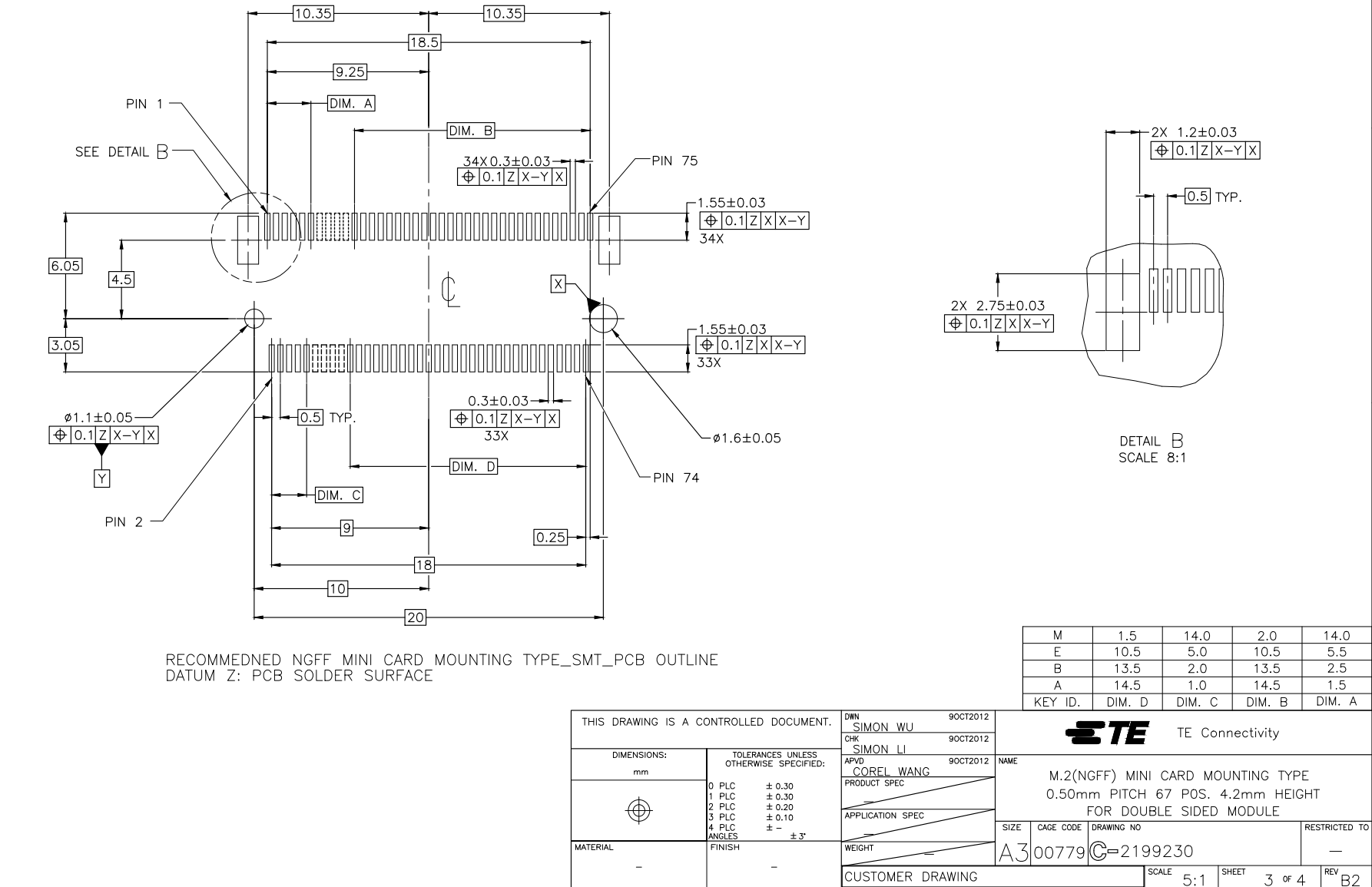
A device, footprint, and symbol for EagleCAD are available in the hardware-libraries Github.
Screw Assembly
The M.2 SoM requires a screw to hold the SoM in place because the M.2 connector does not have integrated locks and the SoM will pop up if not attached to the base board. The screw also provides better vibration resistance than locking clips.
- This is one style of standoff.
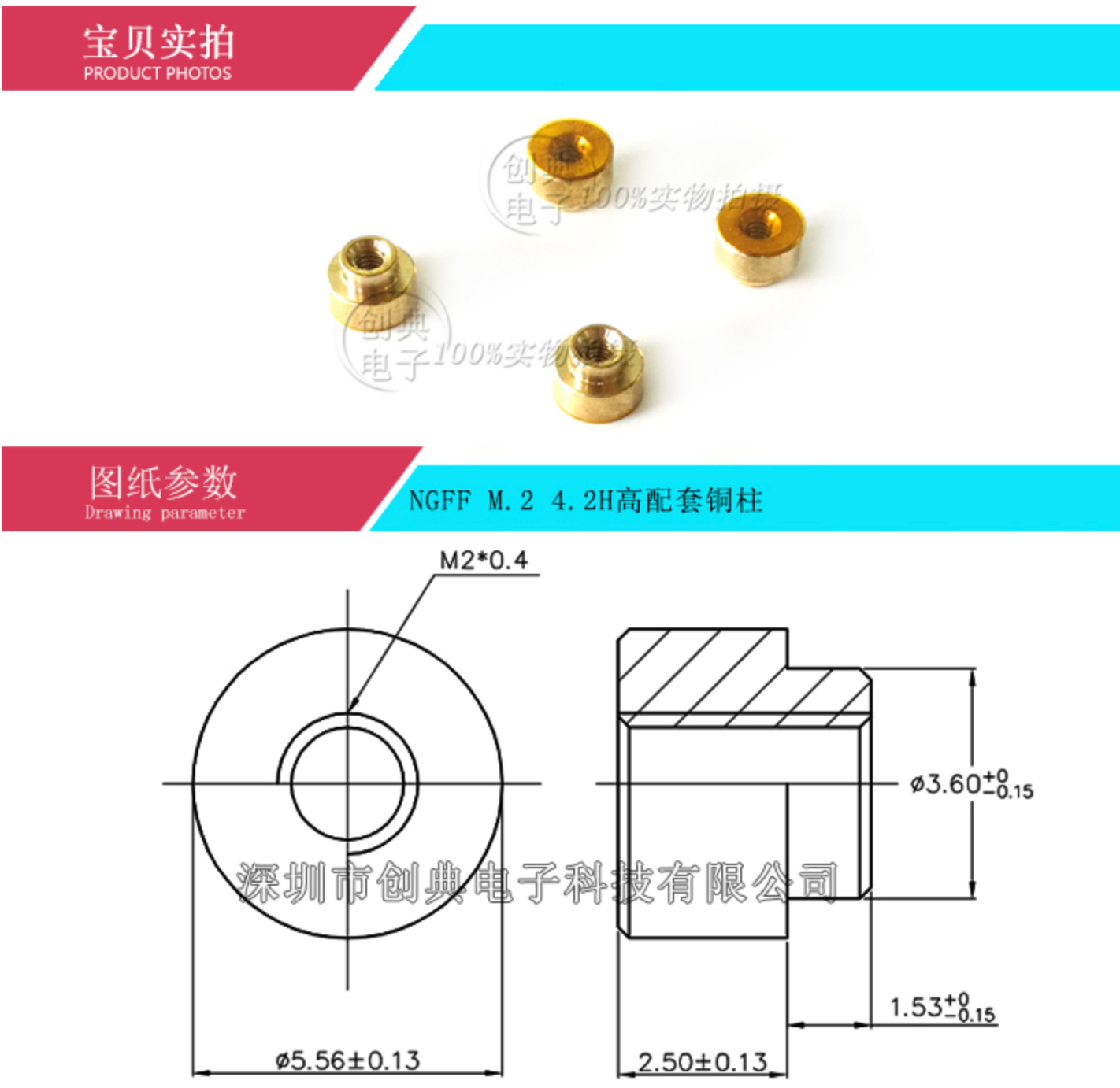
- An alternative design uses a JAE SM3ZS067U410-NUT1-R1200 standoff. It's reflow soldered to your base board and has a threaded hole for a M2*3 screw to hold down the SoM. This may be easier to obtain.
The screw should be connected to the ground plane on your base board.
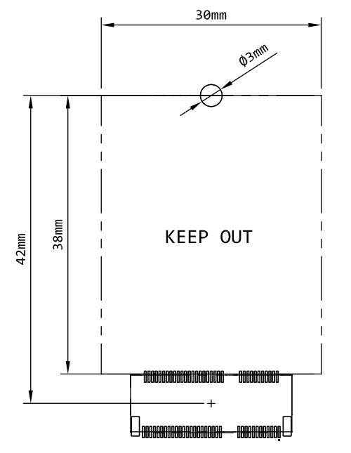
Design Considerations
We strongly recommend against placing components under the SOM board because there is not enough height.
Reference design
The M.2 breakout board design design files for EagleCAD are available as a reference design.
Product Handling
ESD Precautions
The M-SoM contains highly sensitive electronic circuitry and is an Electrostatic Sensitive Device (ESD). Handling an M-SoM without proper ESD protection may destroy or damage it permanently. Proper ESD handling and packaging procedures must be applied throughout the processing, handling and operation of any application that incorporates the Particle M-SoM. ESD precautions should be implemented on the application board where the M-SoM is mounted. Failure to observe these precautions can result in severe damage to the M-SoM!
Connectors
The U.FL antenna connector is not designed to be constantly plugged and unplugged. The antenna pin is static sensitive and you can destroy the radio with improper handling. A tiny dab of glue (epoxy, rubber cement, liquid tape or hot glue) on the connector can be used securely hold the plug in place.
The M.2 edge connector is static sensitive and should be handled carefully. The M.2 connector is not designed for repeated removal and insertion of the module.
Default settings
The M-SoM comes pre-programmed with a bootloader and a user application called Tinker. This application works with an iOS and Android app also named Tinker that allows you to very easily toggle digital pins, take analog and digital readings and drive variable PWM outputs.
The bootloader allows you to easily update the user application via several different methods, USB, OTA, Serial Y-Modem, and also internally via the Factory Reset procedure. All of these methods have multiple tools associated with them as well.
FCC Warnings and End Product Labeling Requirements
Federal Communication Commission Interference Statement
This device complies with Part 15 of the FCC Rules.
This device complies with part 15 of the FCC Rules. Operation is subject to the following two conditions:
(1) This device may not cause harmful interference, and
(2) this device must accept any interference received, including interference that may cause undesired operation.
This equipment has been tested and found to comply with the limits for a Class B digital device, pursuant to part 15 of the FCC Rules. These limits are designed to provide reasonable protection against harmful interference in a residential installation. This equipment generates, uses and can radiate radio frequency energy and, if not installed and used in accordance with the instructions, may cause harmful interference to radio communications. However, there is no guarantee that interference will not occur in a particular installation. If this equipment does cause harmful interference to radio or television reception, which can be determined by turning the equipment off and on, the user is encouraged to try to correct the interference by one or more of the following measures:
- Reorient or relocate the receiving antenna.
- Increase the separation between the equipment and receiver.
- Connect the equipment into an outlet on a circuit different from that to which the receiver is connected.
- Consult the dealer or an experienced radio/TV technician for help.
Any changes or modifications not expressly approved by the party responsible for compliance could void the user's authority to operate this equipment. This transmitter must not be co-located or operating in conjunction with any other antenna or transmitter. This device is intended only for OEM integrators under the following conditions: (For module device use)
(1) The antenna must be installed such that 20 cm is maintained between the antenna and users, and
(2) The transmitter module may not be co-located with any other transmitter or antenna.
As long as 2 conditions above are met, further transmitter test will not be required. However, the OEM integrator is still responsible for testing their end-product for any additional compliance requirements required with this module installed.
Important Notice to OEM integrators - FCC
- This module is limited to OEM installation ONLY.
- This module is limited to installation in mobile applications, according to Part 2.1091(b).
- The separate approval is required for all other operating configurations, including portable configurations with respect to Part 2.1093 and different antenna configurations
- For FCC Part 15.31 (h) and (k): The host manufacturer is responsible for additional testing to verify compliance as a composite system. When testing the host device for compliance with Part 15 Subpart B, the host manufacturer is required to show compliance with Part 15 Subpart B while the transmitter module(s) are installed and operating. The modules should be transmitting and the evaluation should confirm that the Module's intentional emissions are compliant (i.e. fundamental and out of band emissions). The host manufacturer must verify that there are no additional unintentional emissions other than what is permitted in Part 15 Subpart B or emissions are complaint with the transmitter(s) rule(s). The Grantee will provide guidance to the host manufacturer for Part 15 B requirements if needed. Important Note notice that any deviation(s)from the defined parameters of the antenna trace, as described by the instructions, require that the host product manufacturer must notify to Particle that they wish to change the antenna trace design. In this case, a Class II permissive change application is required to be filed by the Particle, or the host manufacturer can take responsibility through the change in FCC ID (new application)procedure followed by a Class II permissive change application.
- This device is certified as a limited module due to lack of shielding. As this device doesn't not have a shield over the radio chip over the radio chip, additional testing and a Class II filing is required for installation in all host devices.
End Product Labeling - FCC
When the module is installed in the host device, the FCC label must be visible through a window on the final device or it must be visible when an access panel, door or cover is easily re-moved. If not, a second label must be placed on the outside of the final device that contains the following text:
M404 for End Product Labeling: The final end product must be labeled in a visible area with the following
Contains FCC ID: 2AEMI-M404
M635 for End Product Labeling: The final end product must be labeled in a visible area with the following
Contains FCC ID: 2AEMI-M635
The FCC ID can be used only when all FCC compliance requirements are met.
Antenna Installation - FCC
(1) The antenna must be installed such that 20 cm is maintained between the antenna and users.
(2) The transmitter module may not be co-located with any other transmitter or antenna.
(3) Only antennas of the same type and with equal or less gains as shown below may be used with this module. Other types of antennas and/or higher gain antennas may require additional authorization for operation.
In the event that these conditions cannot be met (for example certain laptop configurations or co-location with another transmitter), then the FCC authorization is no longer considered valid and the FCC ID cannot be used on the final product. In these circumstances, the OEM integrator will be responsible for re-evaluating the end product (including the transmitter) and obtaining a separate FCC authorization.
To comply with FCC regulations limiting both maximum RF output power and human exposure to RF radiation, Antenna types not included in this list that have a gain greater than the maximum gain indicated for any type listed are strictly prohibited for use with this device:
- 814–849 MHz : 2.01 dBi
- 698–716 MHz: 2.17 dBi
- 703–748 MHz : 2.5 dBi
- 777–787 MHz: 5.3 dBi
- 824–849 MHz: 2.01 dBi
- 1710–1755 MHz: 3.74 dBi
- 1755–1780 MHz : 4 dBi
- 1850–1915 MHz: 5.3 dBi
- 1626.5–1660.5: 3.91 dBi
- 1980–2010 MHz: 4.61dBi
- 2000–2020 MHz:4.37dBi
- BLE:2400 MHz-2483.5 MHz:3dBi
- WiFi:2400MHz-2483.5MHz:3dBi
- WiFi:5150MHz-5850MHz:6.8dBi
Manual Information to the End User - FCC
The OEM integrator has to be aware not to provide information to the end user regarding how to install or remove this RF module in the users manual of the end product which integrates this module. The end user manual shall include all required regulatory information/warning as show in this manual. Radiation Exposure Statement
This equipment complies with FCC radiation exposure limits set forth for an uncontrolled environment. This equipment should be installed and operated with minimum distance 20cm between the radiator & your body.
Outdoor Use - FCC
To be compliant to FCC §15.407(a) the EIRP is not allowed to exceed 125 mW (21 dBm) at any elevation angle above 30° (measured from the horizon) when operated as an outdoor access pointin U-NII-1 band, 5.150-5.250 GHz.
ISED Warnings and End Product Labeling Requirements
Innovation, Science and Economic Development
This device contains licence-exempt transmitter(s)/receiver(s) that comply with Innovation, Science and Economic Development Canada’s licence-exempt RSS(s).
Operation is subject to the following two conditions:
(1) This device may not cause interference;
(2) This device must accept any interference, including interference that may cause undesired operation of the device.
L’émetteur/récepteur exempt de licence contenu dans le présent appareil est conforme aux CNR d’Innovation, Sciences et Développement économique Canada applicables aux appareils radio exempts de licence.
L’exploitation est autorisée aux deux conditions suivantes:
1) L’appareil ne doit pas produire de brouillage;
2) L’appareil doit accepter tout brouillage radioélectrique subi, même si le brouillage est susceptible d’en compromettre le fon-ctionnement.
Radiation Exposure Statement - ISED
This equipment complies with ISED radiation exposure limits set forth for an uncontrolled environment. This equipment should be installed and operated with minimum distance 20cm between the radiator & your body.
Déclaration d'exposition aux radiations
Cet équipement est conforme aux limites d'exposition aux rayonnements ISED établies pour un environnement non contrôlé. Cet équipement doit être installé et utilisé avec un minimum de 20 cm de distance entre la source de rayonnement et votre corps.
This device is intended only for OEM integrators under the following conditions:
1) The antenna must be installed such that 20 cm is maintained between the antenna and users, and
2) The transmitter module may not be co-located with any other transmitter or antenna.
As long as 2 conditions above are met, further transmitter test will not be required. However, the OEM integrator is still responsible for testing their end-product for any additional compliance requirements required with this module installed.
Cet appareil est conçu uniquement pour les intégrateurs OEM dans les conditions suivantes:
1) L'antenne doit être installée de telle sorte qu'une distance de 20 cm est respectée entre l'antenne et les utilisateurs, et
2) Le module émetteur peut ne pas être coïmplanté avec un autre émetteur ou antenne.
Tant que les 2 conditions ci-dessus sont remplies, des essais supplémentaires sur l'émetteur ne seront pas nécessaires. Toutefois, l'intégrateur OEM est toujours responsable des essais sur son produit final pour toutes exigences de conformité supplémentaires requis pour ce module installé.
To comply with ISED regulations limiting both maximum RF output power and human exposure to RF radiation, Antenna types not included in this list that have a gain greater than the maximum gain indicated for any type listed are strictly prohibited for use with this device:
- 824–849 MHz (GSM 850): 2.01 dBi
- 1850–1910 MHz (GSM 1900): 5.3 dBi
- 699–716 MHz (LTE B12): 2.17 dBi
- 703–748 MHz (LTE B28): 2.5 dBi
- 777–787 MHz (LTE B13): 5.3 dBi
- 824–849 MHz (LTE B5): 1.94 dBi
- 1710–1755 MHz (LTE B4): 2.74 dBi
- 1710–1780 MHz (LTE B66): 3.74 dBi
- 1850–1910 MHz (LTE B2): 5.3 dBi
- 1626.5–1660.5 (IOT-NTN B255): 3.91 dBi
- 1980–2010 MHz (IOT-NTN B256): 4.61dBi
- 2000–2020 MHz (IOT-NTN B23): 4.37dBi
- BLE:2400 MHz-2483.5 MHz: 3dBi
- WiFi:2400MHz-2483.5MHz: 3dBi
- WiFi:5150MHz-5850MHz: 6.8dBi
IMPORTANT NOTE:
In the event that these conditions can not be met (for example certain laptop configurations or colocation with another transmitter), then the Canada authorization is no longer considered valid and the IC ID can not be used on the final product. In these circumstances, the OEM integrator will be responsible for re-evaluating the end product (including the transmitter) and obtaining a separate Canada authorization.
NOTE IMPORTANTE:
Dans le cas où ces conditions ne peuvent être satisfaites (par exemple pour certaines configurations d'ordinateur portable ou de certaines co-localisation avec un autre émetteur), l'autorisation du Canada n'est plus considéré comme valide et l'ID IC ne peut pas être utilisé sur le produit final. Dans ces circonstances, l'intégrateur OEM sera chargé de réévaluer le produit final (y compris l'émetteur) et l'obtention d'une autorisation distincte au Canada.
End Product Labeling - ISED
This transmitter module is authorized only for use in device where the antenna may be installed such that 20 cm may be maintained between the antenna and users.
M524 for End Product Labeling: The final end product must be labeled in a visible area with the following:
Contains IC: 20127-M524
M635 for End Product Labeling: The final end product must be labeled in a visible area with the following:
Contains IC: 20127-M635
Plaque signalétique du produit final
Ce module émetteur est autorisé uniquement pour une utilisation dans un dispositif où l'antenne peut être installée de telle sorte qu'une distance de 20cm peut être maintenue entre l'antenne et les utilisateurs. Le produit final doit être étiqueté dans un endroit visible avec l'inscription suivante:
Contient des IC: 20127-M524
Contient des IC: 20127-M635
Manual Information To the End User - ISED
The OEM integrator has to be aware not to provide information to the end user regarding how to install or remove this RF module in the user’s manual of the end product which integrates this module. The end user manual shall include all required regulatory information/warning as show in this manual.
Manuel d'information à l'utilisateur final
L'intégrateur OEM doit être conscient de ne pas fournir des informations à l'utilisateur final quant à la façon d'installer ou de supprimer ce module RF dans le manuel de l'utilisateur du produit final qui intègre ce module. Le manuel de l'utilisateur final doit inclure toutes les informations réglementaires requises et avertissements comme indiqué dans ce manuel.
Outdoor use - ISED
Operation in the band 5150–5250 MHz is only for indoor use to reduce the potential for harmful interference to co-channel mobile satellite systems; Operation in the 5600-5650 MHz band is not allowed in Canada. High-power radars are allocated as primary users (i.e., priority users) of the bands 5250-5350 MHz and 5650-5850 MHz and that these radars could cause interference and/or damage to LE-LAN devices.
Le dispositif de fonctionnement dans la bande 5150-5250 MHz est réservé à une utilisation en intérieur pour réduire le risque d'interférences nuisibles à la co-canal systèmes mobiles par satellite
- Opération dans la bande 5600-5650 MHz n'est pas autorisée au Canada. Haute puissance radars sont désignés comme utilisateurs principaux (c.-àutilisateurs prioritaires) des bandes 5250-5350 MHz et 5650-5850 MHz et que ces radars pourraient causer des interférences et / ou des dommages à dispositifs LAN-EL.
European Union (CE) Warnings and End Product Labeling Requirements
M404 - European Union (CE)
We, Particle Industries, Inc, declare under our sole responsibility that the product, M404, to which this declaration relates, is in conformity with RED Directive 2014/53/EU and (EU) 2015/863 RoHS Directive 2011/65/EU (Recast).
The full text of the EU declaration of conformity is available at the followingInternet address: https://www.particle.io/
Radiation Exposure Statement: This equipment complies with radiation exposure limits set forth for an uncontrolled environment.
The operating frequency bands and the maximum transmitted power limit are listed below:
- BLE 2402-2480MHz 10dBm
- Wi-Fi 2.4GHz band 2412-2484MHz 20dBm
- Wi-Fi 5GHz band 5180-5825MHz 23dBm
- LTE B1 B3 B8 B20 B28 704.5-959.3MHz 1710.7-2687.5 MHz, 25dBm
M524 - European Union (CE)
We, Particle Industries, Inc, declare under our sole responsibility that the product, M524, to which this declaration relates, is in conformity with RED Directive 2014/53/EU and (EU) 2015/863 RoHS Directive 2011/65/EU (Recast).
The full text of the EU declaration of conformity is available at the followingInternet address: https://www.particle.io/
Radiation Exposure Statement: This equipment complies with radiation exposure limits set forth for an uncontrolled environment.
The operating frequency bands and the maximum transmitted power limit are listed below:
- BLE 2402-2480MHz 10dBm
- Wi-Fi 2.4GHz band 2412-2484MHz 20dBm
- Wi-Fi 5GHz band 5180-5825MHz 23dBm
- LTE B1 B3 B7 B8 B20 B28 704.5-959.3MHz 1710.7-2687.5 MHz, 25dBm
- WCDMA 882.4-957.6 MHz 1922.6-2167.4 MHz, 25dBm
- EGSM900 880-915 MHz, 33 dBm
- DCS1800 1710-1785 MHz, 30 dBm
M635e - European Union (CE)
We, Particle Industries, Inc, declare under our sole responsibility that the product, M404, to which this declaration relates, is in conformity with RED Directive 2014/53/EU and (EU) 2015/863 RoHS Directive 2011/65/EU (Recast).
The full text of the EU declaration of conformity is available at the followingInternet address: https://www.particle.io/
Radiation Exposure Statement: This equipment complies with radiation exposure limits set forth for an uncontrolled environment.
The operating frequency bands and the maximum transmitted power limit are listed below:
- BLE 2402-2480MHz 10dBm
- Wi-Fi 2.4GHz band 2412-2484MHz 20dBm
- Wi-Fi 5GHz band 5180-5825MHz 23dBm
- LTE B1 B3 B8 B20 B28 704.5-959.3MHz 1710.7-2687.5 MHz, 25dBm
- EGSM900 880-915 MHz, 33 dBm
- DCS1800 1710-1785 MHz, 30 dBm
United Kingdom
UKCA Conformity:
Radio Equipment Regulations 2017 (S.I. 2017/1206)
Outdoor use (world)
This device is restricted to indoor use when operating in the 5150 to 5350 MHz frequency range. This restriction applies in: AT, BE, BG, CH, CY, CZ, DE, DK, EE, EL, ES, FI, FR, HR, HU, IE, IS, IT, LI, LT, LU, LV, MT, NL, NO, PL, PT, RO, SE, SI, SK, TR, UA, UK(NI).
Certification documents
FCC (United States) - M404 M-SoM M-Series LTE-M/2G
- FCC ID: 2AEMI-M404
- Part 15B
- Part 15C, Digital Transmission System 2.4 GHz
- Part 15E, Unlicensed national information infrastructure TX, 5 GHz
- Part 15B, Part 15 Class B Computing Device Peripheral
- Part 22H, 24E, 27, PCS Licensed Transmitter
ISED (Canada) - M404 M-SoM M-Series LTE-M/2G
- ISED: 20127-M504
- Certificate
- Test Report RS-130
- Test Report RS-132
- Test Report RS-133
- Test Report RS-139
- ICES-003 Issue 7:2020
- Test Report RS-102 (RF Exposure)
CE (European Union) - M404 M-SoM M-Series LTE-M/2G
- Summary
- EN-62368-1 Test Report
- EN 300 328 Test Report BLE (Bluetooth LE 2.4 GHz ISM band)
- EN 300 328 Test Report Wi-Fi (Wi-Fi 2.4 GHz ISM band)
- EN 300 440 Test Report Wi-Fi (Wi-Fi 5 GHz)
- EN 301 893 Test Report Wi-Fi (Wi-Fi 5 GHz)
- EN 301 893 Test Report DFS (Dynamic frequency selection clause 4.2.6)
- EN 303 413 Test Report (GNSS)
- EN 301 489 Test Report
- EN 301 511 Test Report (GSM)
- EN 301 908 Test Report
- EN-62311 Test Report
- Test Report Photos
RoHS - M404 M-SoM M-Series LTE-M/2G
CE (European Union) - M524 M-SoM M-Series LTE Cat 1
- EU Declaration of Conformity (updated 2026-05-18)
- Summary
- EN-62368-1 Test Report
- EN 300 328 Test Report BLE (Bluetooth LE 2.4 GHz ISM band)
- EN 300 328 Test Report Wi-Fi (Wi-Fi 2.4 GHz ISM band)
- EN 301 893 Test Report Wi-Fi (Wi-Fi 5 GHz)
- EN 300 440 Test Report Wi-Fi (Wi-Fi 5 GHz)
- EN 301 893 Test Report DFS (Dynamic frequency selection clause 4.2.6)
- EN 303 413 Test Report (GNSS)
- EN 301 489 Test Report
- EN 301 511 Test Report (GSM)
- EN 301 908 Test Report
- EN-62311 Test Report
- Test Report Photos
RoHS - M524 M-SoM M-Series LTE Cat 1
FCC (United States) - M635e M-SoM M-Series LTE-M/2G/NTN
- FCC ID: 2AEMI-M635
- To be provided at a later date
ISED (Canada) - M635e M-SoM M-Series LTE-M/2G/NTN
- ISED: 20127-M504
- To be provided at a later date
CE (European Union) - M635e M-SoM M-Series LTE Cat M1/2G/NTN
- RED Evaluation
- EMC Test Report
- EN-62368-1 Test Report (safety)
- EN 301 511 Test Report (2G GSM)
- EN 301 908-1 Test Report
- EN 301 908-13 Test Report (4G)
- EN 301 681 Test Report (satellite)
- EN 302 574-3 Test Report (satellite)
- EN 300 328 Test Report - BLE
- EN 300 328 Test Report - Wi-Fi 2.4 GHz
- EN 301 893 Test Report - Wi-Fi 5 GHz
- EN 300 440 Test Report - Wi-Fi 5.8 GHz
- EN 303 413 Test Report (GNSS)
- EN-62311 Test Report
RoHS - M635e M-SoM M-Series LTE Cat M1/2G/NTN
Country compatibility
M404 - Country compatibility
| Country | Model | Technologies | Carriers |
|---|---|---|---|
| Canada | M404 | M1 | Bell Mobility, Rogers Wireless, Telus |
| Mexico | M404 | M1 | AT&T, Telcel |
| United States | M404 | M1 | AT&T, T-Mobile (USA), Verizon7 |
The M404 is fully supported in the United States, Canada, and Mexico. It is in beta testing in other locations. See the carrier list for country compatibility information.
M404 - Certified bands
| Technology | Band | FCC | CE |
|---|---|---|---|
| 2G | 850 MHz | ✓ | |
| 2G | 900 MHz | ||
| 2G | 1800 MHz | ||
| 2G | 1900 MHz | ✓ | |
| LTE Cat M1 | B1 (2100 MHz) | ✓ | |
| LTE Cat M1 | B2 (1900 MHz) | ✓ | |
| LTE Cat M1 | B3 (1800 MHz) | ✓ | |
| LTE Cat M1 | B4 (1700 MHz) | ✓ | |
| LTE Cat M1 | B5 (850 MHz) | ✓ | |
| LTE Cat M1 | B8 (900 MHz) | ✓ | |
| LTE Cat M1 | B12 (700 MHz) | ✓ | |
| LTE Cat M1 | B13 (700 MHz) | ✓ | |
| LTE Cat M1 | B20 (800 MHz) | ✓ | |
| LTE Cat M1 | B25 (1900 MHz) | ✓ | |
| LTE Cat M1 | B26 (850 MHz) | ✓ | |
| LTE Cat M1 | B28 (700 MHz) | ✓ | |
| LTE Cat M1 | B66 (2100 MHz) | ✓ |
M524 - Country compatibility
| Country | Model | Technologies | Carriers |
|---|---|---|---|
| Albania | M524 | 2G, 3G, 4G | Eagle, Telekom, Vodafone |
| Algeria | M524 | 2G, 3G, 4G | Mobilis, Ooredoo |
| Aruba | M524 | 2G, 3G, 4G | Setar |
| Australia | M524 | 4G | Optus, Telstra, Vodafone |
| Austria | M524 | 2G, 4G | 3 (Drei), A1, T-Mobile |
| Bahrain | M524 | 2G, 4G | Zain |
| Bangladesh | M524 | 2G, 3G, 4G | Bangalink, GrameenPhone |
| Belarus | M524 | 2G, 3G, 4G | A1 |
| Belgium | M524 | 2G, 4G | Base, Orange, Proximus |
| Bosnia and Herzegovina | M524 | 2G, 3G | HT Eronet |
| Botswana | M524 | 2G, 3G, 4G | BeMobile |
| Brunei | M524 | 3G, 4G | DST |
| Bulgaria | M524 | 2G, 3G | A1, Telenor, Vivacom |
| Burkina Faso | M524 | 2G, 3G, 4G | Orange |
| Cabo Verde | M524 | 2G, 3G, 4G | CVMóvel, Unitel T+ |
| Cambodia | M524 | 2G, 3G | Metfone |
| Chad | M524 | 2G, 3G, 4G | Airtel |
| Chile | M524 | 3G, 4G | Claro, Entel, Movistar |
| Congo (Brazzaville) | M524 | 2G, 3G, 4G | Airtel |
| Congo (Kinshasa) | M524 | 2G, 3G, 4G | Airtel |
| Côte d'Ivoire | M524 | 2G, 3G | MTN |
| Croatia | M524 | 2G, 3G, 4G | Hrvatski Telekom, Tele2 |
| Cyprus | M524 | 2G, 3G, 4G | MTN, PrimeTel |
| Czechia | M524 | 2G, 4G | O2, T-Mobile, Vodafone |
| Denmark | M524 | 2G, 4G | 3 (Tre), TDC, Telenor, Telia |
| Egypt | M524 | 2G, 3G, 4G | Etisalat, Orange |
| Estonia | M524 | 2G, 3G, 4G | Elisa, Tele2, Telia |
| eSwatini | M524 | 2G, 3G, 4G | MTN |
| Ethiopia | M524 | 2G, 3G, 4G | Ethio Telecom |
| Faroe Islands | M524 | 2G, 3G | Faroese Telecom, Vodafone |
| Finland | M524 | 2G, 4G | DNA, Elisa, Telia |
| France | M524 | 2G, 3G, 4G | Bouygues, Free Mobile, Orange, SFR |
| French Guiana | M524 | 2G, 3G | Digicel |
| Gabon | M524 | 2G, 3G, 4G | Airtel |
| Germany | M524 | 2G, 4G | O2, Telekom, Vodafone |
| Ghana | M524 | 2G, 3G, 4G | AirtelTigo, MTN, Vodafone |
| Gibraltar | M524 | 2G, 3G, 4G | Gibtel |
| Greece | M524 | 2G, 4G | Cosmote, Vodafone, Wind |
| Guinea | M524 | 2G, 3G, 4G | MTN |
| Guinea-Bissau | M524 | 2G, 3G, 4G | MTN |
| Guyana | M524 | 2G | Digicel |
| Hong Kong | M524 | 3G, 4G | CMHK, CSL, SmarTone |
| Hungary | M524 | 2G, 3G, 4G | Magyar Telekom, Telenor, Vodafone |
| Iceland | M524 | 4G | Nova, Siminn, Vodafone |
| Indonesia | M524 | 2G, 4G | Indosat, Telkomsel, XL Axiata |
| Ireland | M524 | 2G, 3G, 4G | 3 (Tre), Meteor, O2, Vodafone |
| Israel | M524 | 4G | Hot Mobile, Orange, Pelephone |
| Italy | M524 | 2G, 4G | TIM, Vodafone, Wind |
| Jordan | M524 | 2G, 3G, 4G | Zain |
| Kazakhstan | M524 | 2G, 3G, 4G | Beeline, K-Cell |
| Kenya | M524 | 2G, 3G, 4G | Airtel |
| Kuwait | M524 | 2G, 3G, 4G | Viva, Zain |
| Latvia | M524 | 2G, 4G | Bite, LMT, Tele2 |
| Liechtenstein | M524 | 2G, 3G, 4G | Mobilkom, Orange |
| Lithuania | M524 | 2G, 4G | Bite, Omnitel, Tele2 |
| Luxembourg | M524 | 2G, 4G | Orange, POST, Tango |
| Macao | M524 | 3G, 4G | CTM |
| Madagascar | M524 | 2G, 3G, 4G | Airtel |
| Malawi | M524 | 2G, 3G, 4G | Airtel |
| Malaysia | M524 | 2G, 4G | Celcom, DiGi, Maxis |
| Malta | M524 | 2G, 3G, 4G | Go Mobile, Vodafone |
| Moldova | M524 | 2G, 3G, 4G | Moldcell, Orange |
| Mongolia | M524 | 2G, 3G | Mobicom, Unitel |
| Montenegro | M524 | 2G, 3G, 4G | Mtel, T-Mobile, Telenor |
| Morocco | M524 | 2G, 3G, 4G | Inwi, Medi Telecom |
| Mozambique | M524 | 2G, 3G, 4G | Vodacom |
| Myanmar | M524 | 2G, 3G, 4G | MPT, Telenor |
| Namibia | M524 | 2G, 3G, 4G | Telecom Namibia |
| Netherlands | M524 | 2G, 3G, 4G | KPN, T-Mobile, Vodafone |
| New Zealand | M524 | 4G | 2degrees, Spark, Vodafone |
| Nigeria | M524 | 2G, 3G, 4G | 9mobile, Airtel, Glo, MTN |
| Norway | M524 | 2G, 3G, 4G | TDC, Telenor, Telia |
| Pakistan | M524 | 2G, 3G, 4G | Mobilink, Telenor, Ufone, Warid |
| Palestine | M524 | 2G, 3G | Jawwal |
| Papua New Guinea | M524 | 2G, 3G | bmobile |
| Poland | M524 | 2G, 3G, 4G | Orange, Play, Plus, T-Mobile |
| Portugal | M524 | 2G, 3G, 4G | NOS, TMN, Vodafone |
| Qatar | M524 | 2G, 4G | Ooredoo, Vodafone |
| Romania | M524 | 2G, 4G | Orange, Telekom Romania, Vodafone |
| Rwanda | M524 | 2G, 3G | Airtel, MTN |
| Serbia | M524 | 2G, 3G, 4G | Telenor, VIP |
| Seychelles | M524 | 2G, 3G, 4G | Airtel |
| Sint Maarten | M524 | 2G, 3G | TelCell |
| Slovakia | M524 | 2G, 4G | O2, Orange, Telekom |
| Slovenia | M524 | 2G, 3G, 4G | A1, Mobitel |
| South Africa | M524 | 2G, 3G, 4G | Cell C, MTN, Vodacom |
| South Korea | M524 | 3G, 4G | KT, LG U+, SK Telecom |
| South Sudan | M524 | 2G, 3G | MTN |
| Spain | M524 | 2G, 3G, 4G | Orange, Telefonica, Vodafone, Yoigo |
| Sri Lanka | M524 | 2G, 4G | Dialog, Mobitel |
| Suriname | M524 | 2G, 3G | Telesur |
| Sweden | M524 | 2G, 4G | 3 (Tre), Tele2, Telenor, Telia |
| Switzerland | M524 | 3G, 4G | Salt, Sunrise, Swisscom |
| Taiwan | M524 | 4G | Chunghwa, FarEasTone, T Star, Taiwan Mobile |
| Tanzania | M524 | 2G, 3G, 4G | Airtel |
| Thailand | M524 | 2G, 3G, 4G | AIS, DTAC, True Move |
| Tunisia | M524 | 2G, 3G, 4G | Orange Tunisie, Tunisie Telecom |
| Uganda | M524 | 2G, 3G, 4G | Africell, Airtel, MTN |
| United Kingdom | M524 | 2G, 4G | 3, EE, O2, Vodafone |
| Vietnam | M524 | 3G, 4G | MobiFone, Viettel, Vinaphone |
| Zambia | M524 | 2G, 3G, 4G | Airtel |
M524 - Certified bands
| Technology | Band | CE |
|---|---|---|
| 2G | 900 MHz | ✓ |
| 2G | 1800 MHz | ✓ |
| 3G | B1 (2100 MHz) | ✓ |
| 3G | B8 (900 MHz) | ✓ |
| LTE Cat 1 | B1 (2100 MHz) | ✓ |
| LTE Cat 1 | B3 (1800 MHz) | ✓ |
| LTE Cat 1 | B7 (2600 MHz) | ✓ |
| LTE Cat 1 | B8 (900 MHz) | ✓ |
| LTE Cat 1 | B20 (800 MHz) | ✓ |
| LTE Cat 1 | B28 (700 MHz) | ✓ |
M635e - Country compatibility
| Country | Model | Technologies | Carriers |
|---|---|---|---|
| Afghanistan | M635E | 2G | MTN |
| Albania | M635E | 2G | Eagle, Telekom, Vodafone |
| Algeria | M635E | 2G | Mobilis, Ooredoo |
| American Samoa | M635E | NTN | Skylo |
| Andorra | M635E | NTN | Skylo |
| Anguilla | M635E | 2G | Flow |
| Antigua and Barbuda | M635E | 2G | Flow |
| Argentina | M635E | 2G, M1 | Claro, Movistar, Personal |
| Armenia | M635E | 2G | Beeline, Ucom |
| Aruba | M635E | 2G | Setar |
| Australia | M635E | M1, NTN | Optus, Skylo, Telstra, Vodafone |
| Austria | M635E | 2G, M1, NTN | 3 (Drei), A1, Skylo, T-Mobile |
| Azerbaijan | M635E | 2G | Azercell, Bakcell, NAR Mobile |
| Bahamas | M635E | 2G | Aliv, BTC Bahamas |
| Bahrain | M635E | 2G | Zain |
| Bangladesh | M635E | 2G | Bangalink |
| Barbados | M635E | 2G | Flow |
| Belarus | M635E | 2G | A1 |
| Belgium | M635E | 2G, M1, NTN | Base, Orange, Proximus, Skylo |
| Bolivia | M635E | 2G | Viva |
| Bosnia and Herzegovina | M635E | 2G | HT Eronet |
| Botswana | M635E | 2G | BeMobile |
| Brazil | M635E | 2G, NTN | Skylo, TIM |
| Bulgaria | M635E | 2G, NTN | A1, Skylo, Telenor, Vivacom |
| Burkina Faso | M635E | 2G | Orange |
| Cabo Verde | M635E | 2G | CVMóvel, Unitel T+ |
| Cambodia | M635E | 2G | Metfone |
| Canada | M635E | M1, NTN | Bell Mobility, Rogers Wireless, Skylo, Telus |
| Cayman Islands | M635E | 2G | Flow |
| Chad | M635E | 2G | Airtel |
| Colombia | M635E | 2G | Movistar |
| Congo (Brazzaville) | M635E | 2G | Airtel |
| Congo (Kinshasa) | M635E | 2G | Airtel |
| Côte d'Ivoire | M635E | 2G | MTN |
| Croatia | M635E | 2G, M1, NTN | Hrvatski Telekom, Skylo, Tele2 |
| Cyprus | M635E | 2G | MTN |
| Czechia | M635E | 2G, NTN | Skylo, T-Mobile, Vodafone |
| Denmark | M635E | 2G, M1, NTN | Skylo, TDC, Telenor, Telia |
| Dominica | M635E | 2G | Flow |
| Dominican Republic | M635E | 2G | Altice Dominicana, Viva |
| Ecuador | M635E | 2G | Claro, Movistar |
| Egypt | M635E | 2G | Etisalat |
| El Salvador | M635E | 2G | Telefonica |
| Estonia | M635E | 2G, M1, NTN | Elisa, Skylo, Tele2, Telia |
| eSwatini | M635E | 2G | MTN |
| Ethiopia | M635E | 2G | Ethio Telecom |
| Faroe Islands | M635E | 2G, NTN | Faroese Telecom, Skylo, Vodafone |
| Finland | M635E | 2G, M1, NTN | DNA, Elisa, Skylo, Telia |
| France | M635E | 2G, M1, NTN | Bouygues, Free Mobile, Orange, SFR, Skylo |
| French Guiana | M635E | 2G | Digicel |
| Gabon | M635E | 2G | Airtel |
| Georgia | M635E | 2G | Beeline, Geocell |
| Germany | M635E | 2G, M1, NTN | O2, Skylo, Telekom, Vodafone |
| Ghana | M635E | 2G | AirtelTigo, MTN |
| Gibraltar | M635E | 2G, NTN | Gibtel, Skylo |
| Greece | M635E | 2G, NTN | Cosmote, Skylo, Wind |
| Grenada | M635E | 2G | Flow |
| Guadeloupe | M635E | 2G | Orange |
| Guatemala | M635E | 2G | Movistar |
| Guernsey | M635E | 2G, NTN | Skylo, Sure |
| Guinea | M635E | 2G | MTN |
| Guinea-Bissau | M635E | 2G | MTN |
| Guyana | M635E | 2G | Digicel |
| Haiti | M635E | 2G | Digicel |
| Holy See (Vatican City) | M635E | NTN | Skylo |
| Honduras | M635E | 2G | Claro, Tigo |
| Hungary | M635E | 2G, M1, NTN | Magyar Telekom, Skylo, Telenor, Vodafone |
| Iceland | M635E | M1, NTN | Nova, Siminn, Skylo, Vodafone |
| India | M635E | 2G | Airtel |
| Indonesia | M635E | 2G | Indosat, Telkomsel, XL Axiata |
| Ireland | M635E | 2G, NTN | Skylo, Vodafone |
| Isle of Man | M635E | 2G, NTN | Manx Telecom, Skylo, Sure |
| Italy | M635E | 2G, NTN | Skylo, TIM, Vodafone, Wind |
| Japan | M635E | M1, NTN | KDDI, NTT DoCoMo, Skylo, Softbank |
| Jersey | M635E | 2G, NTN | Jersey Telecom, Skylo, Sure |
| Jordan | M635E | 2G | Zain |
| Kazakhstan | M635E | 2G | Beeline, K-Cell |
| Kenya | M635E | 2G | Airtel |
| Kosovo | M635E | NTN | Skylo |
| Kuwait | M635E | 2G | Viva, Zain |
| Kyrgyzstan | M635E | 2G | Beeline |
| Latvia | M635E | 2G, M1, NTN | Bite, LMT, Skylo, Tele2 |
| Liechtenstein | M635E | 2G, NTN | Mobilkom, Orange, Skylo |
| Lithuania | M635E | 2G, M1, NTN | Bite, Omnitel, Skylo, Tele2 |
| Luxembourg | M635E | 2G, M1, NTN | Orange, POST, Skylo, Tango |
| Madagascar | M635E | 2G | Airtel |
| Malawi | M635E | 2G | Airtel |
| Malaysia | M635E | 2G | DiGi, Maxis |
| Malta | M635E | 2G, M1, NTN | Go Mobile, Skylo |
| Mexico | M635E | M1, NTN | AT&T, Skylo, Telcel |
| Moldova | M635E | 2G | Moldcell, Orange |
| Monaco | M635E | NTN | Skylo |
| Mongolia | M635E | 2G | Mobicom, Unitel |
| Montenegro | M635E | 2G | T-Mobile, Telenor |
| Morocco | M635E | 2G | Inwi, Medi Telecom |
| Mozambique | M635E | 2G | Vodacom |
| Myanmar | M635E | 2G | MPT |
| Namibia | M635E | 2G | Telecom Namibia |
| Netherlands | M635E | 2G, M1, NTN | KPN, Skylo, T-Mobile, Vodafone |
| New Zealand | M635E | M1, NTN | Skylo, Spark, Vodafone |
| Nicaragua | M635E | 2G | Movistar |
| Nigeria | M635E | 2G | 9mobile, Airtel, Glo |
| North Macedonia | M635E | 2G, NTN | Skylo, Vip operator |
| Norway | M635E | 2G, M1, NTN | Skylo, TDC, Telenor, Telia |
| Oman | M635E | 2G | Ooredoo |
| Pakistan | M635E | 2G | Mobilink, Ufone, Warid |
| Palestine | M635E | 2G | Jawwal |
| Panama | M635E | 2G | Movistar |
| Papua New Guinea | M635E | 2G | bmobile |
| Paraguay | M635E | 2G | Personal, Tigo, Vox |
| Peru | M635E | 2G | Entel |
| Philippines | M635E | 2G | Globe, Smart |
| Poland | M635E | 2G, M1, NTN | Orange, Play, Plus, Skylo, T-Mobile |
| Portugal | M635E | 2G, M1, NTN | NOS, Skylo, TMN, Vodafone |
| Puerto Rico | M635E | NTN | Skylo |
| Qatar | M635E | 2G | Ooredoo, Vodafone |
| Romania | M635E | 2G, M1, NTN | Orange, Skylo, Telekom Romania, Vodafone |
| Russia | M635E | 2G | Beeline, Megafon, MTS, Tele2 |
| Rwanda | M635E | 2G | Airtel, MTN |
| Saint Kitts and Nevis | M635E | 2G | Flow |
| Saint Lucia | M635E | 2G | Flow |
| San Marino | M635E | NTN | Skylo |
| Serbia | M635E | 2G | Telenor, VIP |
| Seychelles | M635E | 2G | Airtel |
| Singapore | M635E | M1 | SingTel |
| Sint Maarten | M635E | 2G | TelCell |
| Slovakia | M635E | 2G, M1, NTN | O2, Orange, Skylo, Telekom |
| Slovenia | M635E | 2G, M1, NTN | A1, Mobitel, Skylo |
| South Africa | M635E | 2G | Cell C, MTN, Vodacom |
| South Korea | M635E | M1 | KT, SK Telecom |
| South Sudan | M635E | 2G | MTN |
| Spain | M635E | 2G, M1, NTN | Orange, Skylo, Telefonica, Vodafone, Yoigo |
| Suriname | M635E | 2G | Telesur |
| Sweden | M635E | 2G, M1, NTN | 3 (Tre), Skylo, Tele2, Telenor, Telia |
| Switzerland | M635E | M1, NTN | Salt, Skylo, Sunrise, Swisscom |
| Taiwan | M635E | M1 | Chunghwa |
| Tajikistan | M635E | 2G | Beeline, Tcell |
| Tanzania | M635E | 2G | Airtel |
| Trinidad and Tobago | M635E | 2G | TSTT |
| Tunisia | M635E | 2G | Orange Tunisie, Tunisie Telecom |
| Turks and Caicos Islands | M635E | 2G | Flow |
| Uganda | M635E | 2G | Africell, Airtel, MTN |
| Ukraine | M635E | 2G | Kyivstar, Life, MTS |
| United Arab Emirates | M635E | M1 | Etisalat |
| United Kingdom | M635E | 2G, M1, NTN | EE, O2, Skylo, Vodafone |
| United States | M635E | M1, NTN | AT&T, Skylo, T-Mobile (USA), Verizon7 |
| Uruguay | M635E | 2G | Antel |
| Uzbekistan | M635E | 2G | Beeline |
| Virgin Islands (British) | M635E | 2G | CCT, Flow |
| Zambia | M635E | 2G | Airtel |
M635e - Certified bands
| Technology | Band | FCC | CE |
|---|---|---|---|
| 2G | 850 MHz | ✓ | |
| 2G | 900 MHz | ||
| 2G | 1800 MHz | ||
| 2G | 1900 MHz | ✓ | |
| LTE Cat M1 | B1 (2100 MHz) | ✓ | |
| LTE Cat M1 | B2 (1900 MHz) | ✓ | |
| LTE Cat M1 | B3 (1800 MHz) | ✓ | |
| LTE Cat M1 | B4 (1700 MHz) | ✓ | |
| LTE Cat M1 | B5 (850 MHz) | ✓ | |
| LTE Cat M1 | B8 (900 MHz) | ✓ | |
| LTE Cat M1 | B12 (700 MHz) | ✓ | |
| LTE Cat M1 | B13 (700 MHz) | ✓ | |
| LTE Cat M1 | B18 (850 MHz)1 | ||
| LTE Cat M1 | B19 (850 MHz)1 | ||
| LTE Cat M1 | B20 (800 MHz) | ✓ | |
| LTE Cat M1 | B25 (1900 MHz) | ✓ | |
| LTE Cat M1 | B26 (850 MHz) | ✓ | |
| LTE Cat M1 | B27 (800 MHz) | ||
| LTE Cat M1 | B28 (700 MHz) | ✓ | |
| LTE Cat M1 | B66 (2100 MHz) | ✓ | |
| LTE Cat M1 | B85 (700 MHz) | ||
| IoT NTN | n255 (1.6 GHz) | ✓ | ✓ |
| IoT NTN | n256 (2.0 GHz) | ✓ | ✓ |
- 1B18 and B19 are used only in Japan
Ordering information
| SKU | Description | Region | Modem | EtherSIM | Lifecycle | Replacement |
|---|---|---|---|---|---|---|
| M404MEA | M-Series LTE-M/2G (Global, EtherSIM), [x1] | Global | BG95-M5 | ✓ | GA | |
| M404MTY | M-Series LTE-M/2G (Global, EtherSIM), Tray [x50] | Global | BG95-M5 | ✓ | GA | |
| M524MEA | M-Series LTE CAT1/3G/2G (Europe, EtherSIM), [x1] | EMEAA | EG91-EX | ✓ | GA | |
| M524MTY | M-Series LTE CAT1/3G/2G (Europe, EtherSIM), Tray [x50] | EMEAA | EG91-EX | ✓ | GA | |
| M635EMEA | M-Series LTE M1/2G/Satellite Kit (Global, EtherSIM), [x1] | Global | BG95-S5 | ✓ | In development |
- EMEAA: Selected countries in Europe, Middle East, Africa, and Asia, including Australia and New Zealand. See the cellular carrier list for more information.
Revision history
| Revision | Date | Author | Comments |
|---|---|---|---|
| pre | 2023-10-03 | RK | Initial version |
| 2023-12-20 | RK | Added FCC and IC IDs. Additional notes for ADCs, D24, and D25 | |
| 2024-02-08 | RK | Added power consumption information | |
| 2024-02-20 | RK | M.2 screw assembly should be connected to ground | |
| 2024-02-20 | RK | Added pin drive strength | |
| 2024-03-14 | RK | M SoM pin 45 is not shared. Pins 43 and 53 are both connected to PB[2], but not pin 45. | |
| 2024-03-15 | RK | The UART baud rate 2400, 4800, 380400, 460800 are supported but were not listed | |
| 2024-03-26 | RK | Listed certified bands for FCC and CE | |
| 001 | 2024-04-02 | RK | General availability |
| 002 | 2024-04-03 | RK | Additional transmitter information |
| 003 | 2024-04-18 | RK | Add PDM microphone |
| 004 | 2024-04-23 | RK | Added links to certification documents |
| 005 | 2024-04-25 | RK | Added I/O characteristics |
| 006 | 2024-04-30 | RK | Corrected SPI interface speeds |
| 007 | 2024-07-09 | RK | Updated cellular modem on M635 to BG95-S5 |
| 008 | 2024-08-21 | RK | Added supervisory reset information |
| 009 | 2024-09-03 | RK | Added clarification of cellular modem USB pins |
| 010 | 2024-09-24 | RK | Removed concurrent GNSS warning, added link to library |
| 011 | 2024-10-02 | RK | Added warning to not use Argon (ANT-FLXV2) antenna |
| 012 | 2025-01-06 | RK | Added note explaining reserved SoM pins |
| 013 | 2025-01-21 | RK | Incorrect RTL pin listed in SETUP and RESET button section. It was listed as PA[4] but is PA[11]. It was correct in the pin diagram. |
| 014 | 2025-04-10 | RK | Added links to hardware-libraries and M.2 breakout board designs |
| 015 | 2025-06-25 | RK | Clarifications for GNSS use |
| 016 | 2026-05-18 | RK | Updated EU Declaration of Conformity |
| 017 | 2026-06-09 | RK | Updated bands and country list for M635e |
| 018 | 2026-06-15 | RK | Added NTN antenna information |
| 019 | 2026-06-17 | RK | Updates for M635e certification |
| 020 | 2026-07-09 | RK | Updates for M635e certification |