
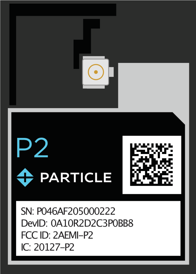
P2 Datasheet
Functional description
Overview
The P2 is a SMD module with a microcontroller and Wi-Fi networking. The form-factor is the same as the P1, but the P2 supports 2.4 GHz and 5 GHz Wi-Fi, BLE, and has much larger RAM and flash that can support larger applications.
Features
- 802.11a/b/g/n Wi-Fi, 2.4 GHz and 5 GHz
- Integrated PCB antenna
- Integrated U.FL connector for external antenna
- Integrated RF switch
- BLE 5 using same antenna as Wi-Fi
- Realtek RTL8721DM MCU
- ARM Cortex M33 CPU, 200 MHz
- 2048 KB (2 MB) user application maximum size
- 3072 KB (3 MB) of RAM available to user applications
- 2 MB flash file system
- FCC (United States), ISED (Canada), and CE (European Union) certified
Device OS support
The P2 requires Device OS 5.0.0 or later. It is recommended that you use the latest version in the 5.x release line.
Some P2 devices from the factory shipped with Device OS 3.2.1-p2.3. This version should not be used in production.
For information on upgrading Device OS, see Version information. For the latest version shipped from the factory, see Manufacturing firmware versions page. See also Long Term Support (LTS) releases.
Interfaces
Block diagram
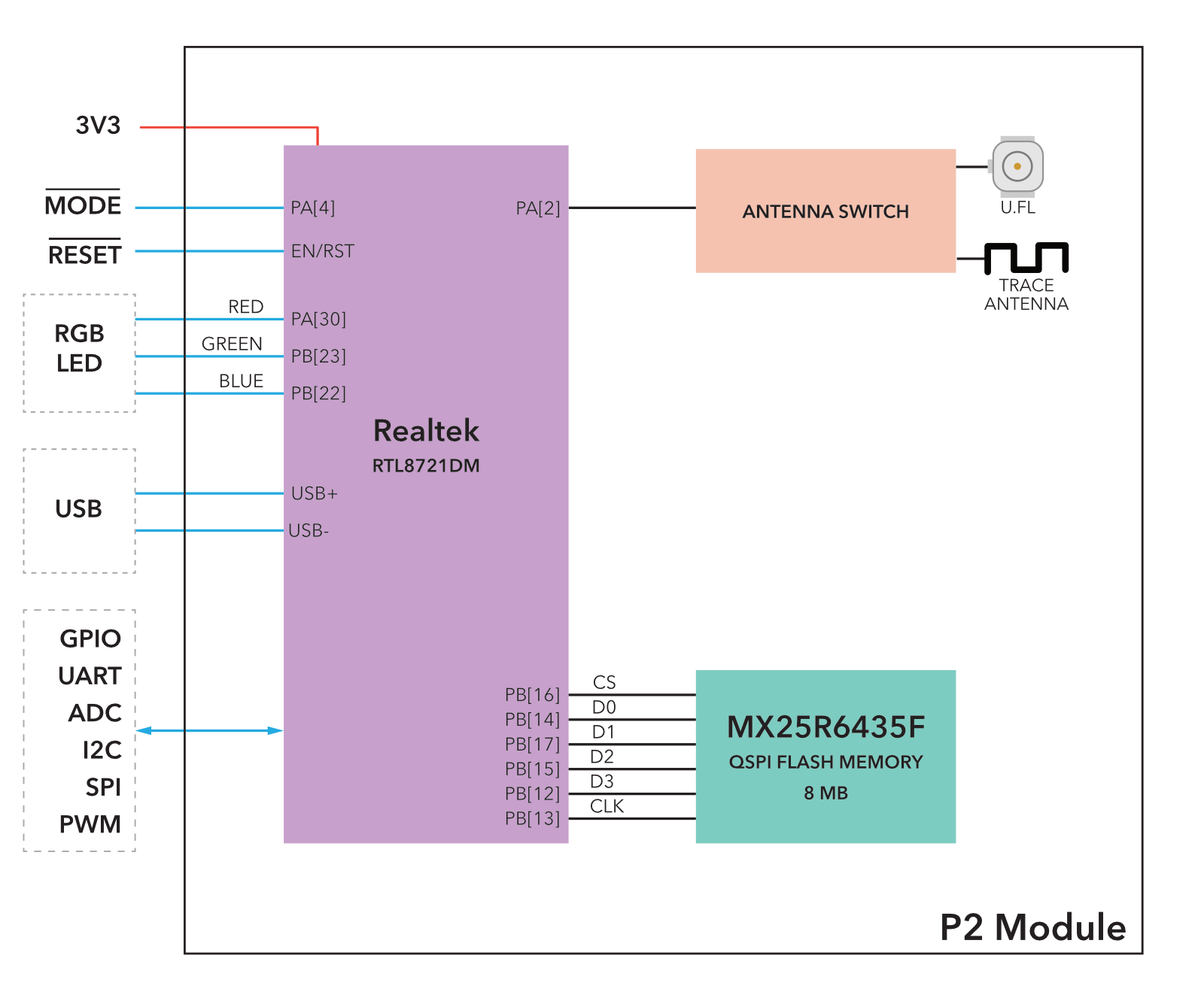
RF
- The P2 includes an on-module PCB trace antenna and a U.FL connector that allows the user to connect an external antenna.
- The antenna is selected in software. The default is the PCB trace antenna.
- The area surrounding the PCB antenna on the carrier PCB should be free of ground planes and signal traces for maximum Wi-Fi performance when using the trace antenna.
- Device operation in the 5150-5250 MHz band is only for indoor use to reduce the potential for harmful interference to co-channel mobile satellite systems.
Approved antennas
In addition to the built-in trace antenna, the following optional external antenna is certified for use with the P2:
| Antenna | SKU |
|---|---|
| Particle P2/Photon2 Wi-Fi Antenna 2.4/5GHz, [x1] | PARANTWM1EA |
| Particle P2/Photon2 Wi-Fi Antenna 2.4/5GHz, [x50] | PARANTWM1TY |
This antenna is used for both Wi-Fi and BLE. In order to use an external antenna, it must be selected in software.
A different dual-band antenna can be used but this will likely require both intentional and unintentional radiator certification.
Do not use the Argon Wi-Fi/BLE antenna (ANT-FLXV2) on the P2, Photon 2, or M-SoM. The Argon antenna does not work with 5 GHz and this will result in poor Wi-Fi performance on the P2, Photon 2, and M-SoM.
SWD/JTAG
The P2 module supports programming and debugging use SWD (Serial Wire Debug) on pins D6 and D7.
| Pin | JTAG | MCU Pin | P2 Pin # | Pull at boot |
|---|---|---|---|---|
| D7 | SWDIO | PA[27] | 54 | Pull-up |
| D6 | SWCLK | PB[3] | 55 | Pull-down |
| 3V3 | Power | |||
| GND | Ground | |||
| RST | Reset |
When the bootloader starts, for a brief period of time a weak pull-up is applied to pin D7 and pull-down to pin D6 to detect whether a SWD debugger is attached. After boot, you can use these pins for regular GPIO, but beware of a possible GPIO state change caused by the pull-up or pull-down when using these pins as output.
Note that SWD is shared with GPIO pins D6 and D7, and by default SWD is only enabled while the bootloader is running, immediately at boot, and when in DFU mode (blinking yellow). Only Debug builds in Particle Workbench have SWD enabled in when user firmware is running.
3V3
3V3 is used to supply power to RTL8721 MCU, Wi-Fi, memory, etc.. 3.3V at a minimum of 500 mA is required.
These limits do not include any 3.3V peripherals on your base board, so that may increase the current requirements.
Power supply requirements:
- 3.3V output
- Maximum 5% voltage drop
- 100 mV peak-to-peak ripple maximum
- 500 mA minimum output current at 3.3V recommended for future compatibility
- Maintain these values at no-load as well as maximum load
In some cases, it may be necessary to add a supervisory/reset IC, such as the Richtek RT9818C or SG Micro SGM809-RXN3L/TR:
- If your power supply has a slew rate from 1.5V to 3.0V slower than 15 ms, a reset IC is required.
- If your power supply at power off cannot be guaranteed to drop below 0.3V before powering back up, a reset IC required.
See supervisory reset, below, for additional information.
Memory map
Flash layout overview
| Address | File | Purpose |
|---|---|---|
| 0x00000000 | p2-prebootloader-mbr | This file is factory configured and must never be overwritten |
| 0x00004000 | p2-bootloader | Device OS bootloader |
| 0x00014000 | p2-prebootloader-part1 | Bootloader for KM0 processor, infrequently modified |
| 0x00060000 | p2-system-part1 | Device OS system part |
The location of the user binary is dependent on the size of the user binary and is not flashed to a fixed location.
Do not chip erase the RTL872x under any circumstances! Also do not flash anything to address 0 (prebootloader-mbr). The prebootloader-mbr is factory configured for your specific device with the private keys necessary for secure boot. If you erase or overwrite this portion of the flash you will not be able to program or use the device again.
DCT Layout
The DCT area of flash memory has been mapped to a separate DFU media device so that we can incrementally update the application data. This allows one item (say, server public key) to be updated without erasing the other items.
| Region | Offset | Size |
|---|---|---|
| system flags | 0 | 32 |
| version | 32 | 2 |
| device private key | 34 | 1216 |
| device public key | 1250 | 384 |
| ip config | 1634 | 120 |
| feature flags | 1754 | 4 |
| country code | 1758 | 4 |
| claim code | 1762 | 63 |
| claimed | 1825 | 1 |
| ssid prefix | 1826 | 26 |
| device code | 1852 | 6 |
| version string | 1858 | 32 |
| dns resolve | 1890 | 128 |
| reserved1 | 2018 | 64 |
| server public key | 2082 | 768 |
| padding | 2850 | 2 |
| flash modules | 2852 | 100 |
| product store | 2952 | 24 |
| antenna selection | 2976 | 1 |
| cloud transport | 2977 | 1 |
| alt device public key | 2978 | 128 |
| alt device private key | 3106 | 192 |
| alt server public key | 3298 | 192 |
| alt server address | 3490 | 128 |
| device id | 3618 | 12 |
| radio flags | 3630 | 1 |
| mode button mirror | 3631 | 32 |
| led mirror | 3663 | 96 |
| led theme | 3759 | 64 |
| reserved2 | 3823 | 435 |
Pin and button definition
| Peripheral Type | Qty | Input(I) / Output(O) |
|---|---|---|
| Digital | 22 | I/O |
| Analog (ADC) | 6 | I |
| SPI | 2 | I/O |
| I2C | 1 | I/O |
| UART | 3 | I/O |
| USB | 1 | I/O |
| PWM | 5 | O |
Pin markings
GPIO (Digital I/O)
| Pin | P2 Pin Name | P2 GPIO | MCU | Special boot function |
|---|---|---|---|---|
| 23 | A5 / D14 | ✓ | PB[4] | |
| 30 | D10 / WKP | ✓ | PA[15] | |
| 33 | S6 / D21 | ✓ | PB[31] | |
| 35 | D1 / A4 | ✓ | PB[5] | |
| 36 | D0 / A3 | ✓ | PB[6] | |
| 40 | S0 / D15 | ✓ | PA[12] | |
| 41 | S1 / D16 | ✓ | PA[13] | |
| 42 | S2 / D17 | ✓ | PA[14] | |
| 43 | A1 / D12 | ✓ | PB[2] | |
| 44 | S3 / D18 | ✓ | PB[26] | |
| 45 | D2 | ✓ | PA[16] | |
| 47 | S4 / D19 | ✓ | PA[0] | |
| 49 | A2 / D13 | ✓ | PB[7] | |
| 50 | A0 / D11 | ✓ | PB[1] | |
| 51 | D3 | ✓ | PA[17] | |
| 52 | D4 | ✓ | PA[18] | |
| 53 | D5 | ✓ | PA[19] | |
| 54 | D7 | ✓ | PA[27] | SWDIO. 40K pull-up at boot. Low at boot triggers MCU test mode. |
| 55 | D6 | ✓ | PB[3] | SWCLK. 40K pull-down at boot. |
| 63 | RX / D9 | ✓ | PA[8] | |
| 64 | TX / D8 | ✓ | PA[7] | Low at boot triggers ISP flash download |
- The drive strength is 4 mA per pin in normal drive and 12 mA per pin in high drive mode on the P2.
- There is a maximum of 200 mA across all pins. The total maximum could be further limited by your 3.3V regulator.
- Drive strength selection using pinSetDriveStrength is only available in Device OS 5.5.0 and later on the P2.
- On the P2, Pin RGBR (PA[30]) has a 10K hardware pull-up in the module because it's a trap pin that controls the behavior of the internal 1.1V regulator. This does not affect the RGB LED but could affect your design if you are repurposing this pin as GPIO. You must not hold this pin low at boot.
- Pins TX, D6, and D7 have additional limitations, see boot mode pins, below.
ADC (analog to digital converter)
The P2 supports six ADC inputs.
| Pin | Pin Name | Description | Interface | MCU |
|---|---|---|---|---|
| 23 | A5 / D14 | A5 Analog in, GPIO, PWM. | ADC_0 | PB[4] |
| 35 | D1 / A4 | D1 GPIO, PWM, I2C SCL, A4 Analog In | ADC_1 | PB[5] |
| 36 | D0 / A3 | D0 GPIO, I2C SDA, A3 Analog In | ADC_2 | PB[6] |
| 43 | A1 / D12 | A1 Analog in, PDM DAT, GPIO | ADC_5 | PB[2] |
| 49 | A2 / D13 | A2 Analog in, PWM, GPIO | ADC_3 | PB[7] |
| 50 | A0 / D11 | A0 Analog in, PDM CLK, GPIO | ADC_4 | PB[1] |
- ADC inputs are single-ended and limited to 0 to 3.3V
- Resolution is 12 bits
The ADCs on the P2 and Photon 2 (RTL872x) have a lower impedance than other Particle device MCUs (nRF52, STM32F2xx). They require a stronger drive and this may cause issues when used with a voltage divider.
For signals that change slowly, such as NTC thermocouple resistance, you can add a 2.2 uF capacitor to the signal. For rapidly changing signals, a voltage follower IC can be used.
VBAT_MEAS (A6)
The VBAT_MEAS pin is connected to Li+ on the Photon 2 and is used to measure the battery voltage by using analogRead(A6). The value returned is 0 - 4095 (inclusive, 12-bit) but represents voltage from 0 - 5 VDC, not 3.3V as is the case with the other ADC inputs.
This pin can be used as an ADC on the P2 with a range of 0 - 5 VDC, however because of the built-in voltage divider combined with the high impedance of the RTL872x ADCs, there may be issues if your circuit does not have sufficient drive, or also includes a voltage divider.
UART serial
The P2 supports three UART serial interfaces.
| Pin | Pin Name | Description | Interface | MCU |
|---|---|---|---|---|
| 30 | D10 / WKP | D10 GPIO, Serial 3 CTS, WKP. (Was WKP/A7 on P1.) | Serial3 (CTS) | PA[15] |
| 40 | S0 / D15 | S0 GPIO, PWM, SPI MOSI, Serial3 TX, I2S MCLK. (Was P1S0 on P1.) | Serial3 (TX) | PA[12] |
| 41 | S1 / D16 | S1 GPIO, PWM, SPI MISO, Serial3 RX. (Was P1S1 on P1.) | Serial3 (RX) | PA[13] |
| 42 | S2 / D17 | S2 GPIO, SPI SCK, Serial3 RTS. (Was P1S2 on P1.) | Serial3 (RTS) | PA[14] |
| 45 | D2 | D2 GPIO, Serial2 RTS, SPI1 MOSI | Serial2 (RTS) | PA[16] |
| 51 | D3 | D3 GPIO, Serial2 CTS, SPI1 MISO | Serial2 (CTS) | PA[17] |
| 52 | D4 | D4 GPIO, Serial2 TX, SPI1 SCK | Serial2 (TX) | PA[18] |
| 53 | D5 | D5 GPIO, Serial2 RX, SPI1 SS | Serial2 (RX) | PA[19] |
| 63 | RX / D9 | Serial1 RX (received data), GPIO | Serial1 (RX) | PA[8] |
| 64 | TX / D8 | Serial1 TX (transmitted data), GPIO | Serial1 (TX) | PA[7] |
- The UART pins are 3.3V and must not be connected directly to a RS-232C port or to a 5V TTL serial port
- Hardware flow control is optional; if not used then the RTS and CTS pins can be used as regular GPIO
- Serial1 uses the RTL872x UART_LOG peripheral
- Serial2 uses the RTL872x HS_UART0 peripheral
- Serial3 uses the RTL872x LP_UART peripheral
- Supported baud rates: 110, 300, 600, 1200, 2400, 4800, 9600, 14400, 19200, 28800, 38400, 57600, 76800, 115200, 128000, 153600, 230400, 380400, 460800, 500000, 921600, 1000000, 1382400, 1444400, 1500000, 1843200, 2000000, 2100000, 2764800, 3000000, 3250000, 3692300, 3750000, 4000000, 6000000
SPI
The P2 supports two SPI (serial peripheral interconnect) ports.
| Pin | Pin Name | Description | Interface | MCU |
|---|---|---|---|---|
| 40 | S0 / D15 | S0 GPIO, PWM, SPI MOSI, Serial3 TX, I2S MCLK. (Was P1S0 on P1.) | SPI (MOSI) | PA[12] |
| 41 | S1 / D16 | S1 GPIO, PWM, SPI MISO, Serial3 RX. (Was P1S1 on P1.) | SPI (MISO) | PA[13] |
| 42 | S2 / D17 | S2 GPIO, SPI SCK, Serial3 RTS. (Was P1S2 on P1.) | SPI (SCK) | PA[14] |
| 44 | S3 / D18 | S3 GPIO, I2S TX. (Was P1S3 on P1.), SPI SS | SPI (SS) | PB[26] |
| 45 | D2 | D2 GPIO, Serial2 RTS, SPI1 MOSI | SPI1 (MOSI) | PA[16] |
| 51 | D3 | D3 GPIO, Serial2 CTS, SPI1 MISO | SPI1 (MISO) | PA[17] |
| 52 | D4 | D4 GPIO, Serial2 TX, SPI1 SCK | SPI1 (SCK) | PA[18] |
| 53 | D5 | D5 GPIO, Serial2 RX, SPI1 SS | SPI1 (SS) | PA[19] |
- The SPI port is 3.3V and must not be connected directly to devices that drive MISO at 5V
- If not using a SPI port, its pins can be used as GPIO
- Any pins can be used as the SPI chip select
- Multiple devices can generally share a single SPI port
- SPI uses the RTL872x SPI1 peripheral (25 MHz maximum speed)
- SPI1 uses the RTL872x SPI0 peripheral (50 MHz maximum speed)
If you are using SPI, Device OS 5.3.1 or later is recommended. Prior to that version, SPI ran at half of the set speed, and SPI1 ran at double the set speed. Timing has also been improved for large DMA transfers; prior to 5.3.1, there could be 1 µs gaps for every 16 bytes of data transferred.
I2C
The P2 supports one I2C (two-wire serial interface) port.
| Pin | Pin Name | Description | Interface | MCU |
|---|---|---|---|---|
| 35 | D1 / A4 | D1 GPIO, PWM, I2C SCL, A4 Analog In | Wire (SCL) | PB[5] |
| 36 | D0 / A3 | D0 GPIO, I2C SDA, A3 Analog In | Wire (SDA) | PB[6] |
- The I2C port is 3.3V and must not be connected directly a 5V I2C bus
- Maximum bus speed is 400 kHz
- External pull-up resistors are required for I2C
- If not using I2C, pins D0 and D1 can be used as GPIO or analog input.
PWM
The P2 supports PWM (pulse-width modulation) on the following pins:
| Pin | Pin Name | Description | MCU |
|---|---|---|---|
| 23 | A5 / D14 | A5 Analog in, GPIO, PWM. | PB[4] |
| 35 | D1 / A4 | D1 GPIO, PWM, I2C SCL, A4 Analog In | PB[5] |
| 40 | S0 / D15 | S0 GPIO, PWM, SPI MOSI, Serial3 TX, I2S MCLK. (Was P1S0 on P1.) | PA[12] |
| 41 | S1 / D16 | S1 GPIO, PWM, SPI MISO, Serial3 RX. (Was P1S1 on P1.) | PA[13] |
| 49 | A2 / D13 | A2 Analog in, PWM, GPIO | PB[7] |
All available PWM pins on the P2 share a single timer. This means that they must all share a single frequency, but can have different duty cycles.
PDM
Pulse density modulation digital microphones can be used with the Microphone_PDM library and the P2, but only on specific pins:
| Pin | Pin Name | Description | MCU |
|---|---|---|---|
| 43 | A1 / D12 | A1 Analog in, PDM DAT, GPIO | PB[2] |
| 50 | A0 / D11 | A0 Analog in, PDM CLK, GPIO | PB[1] |
USB
The P2 supports a USB interface for programming the device and for USB serial (CDC) communications. The module itself does not contain a USB connector; you typically add a micro USB or USB C connector on your base board. It is optional but recommended.
| Pin | Pin Name | Description | MCU |
|---|---|---|---|
| 61 | USBDATA+ | USB Data+ | PA[26] |
| 62 | USBDATA- | USB Data- | PA[25] |
RGB LED
The P2 supports an external common anode RGB LED.
One common LED that meets the requirements is the Cree CLMVC-FKA-CL1D1L71BB7C3C3 which is inexpensive and easily procured. You need to add three current limiting resistors. With this LED, we typically use 1K ohm current limiting resistors. These are much larger than necessary. They make the LED less blinding but still provide sufficient current to light the LEDs. If you want maximum brightness you should use the calculated values - 33 ohm on red, and 66 ohm on green and blue.
A detailed explanation of different color codes of the RGB system LED can be found here.
The use of the RGB LED is optional, however it is highly recommended as troubleshooting the device without the LED is very difficult.
| Pin | Pin Name | Description | MCU |
|---|---|---|---|
| 29 | RGBR | RGB LED Red. Has 10K hardware pull-up. Do not hold low at boot. | PA[30] |
| 31 | RGBB | RGB LED Blue | PB[22] |
| 32 | RGBG | RGB LED Green | PB[23] |
- On the P2, Pin RGBR (PA[30]) has a 10K hardware pull-up in the module because it's a trap pin that controls the behavior of the internal 1.1V regulator. This does not affect the RGB LED but could affect your design if you are repurposing this pin as GPIO. You must not hold this pin low at boot.
Boot mode pins
These pins have a special function at boot. Beware when using these pins as input as they can trigger special modes in the MCU.
| Pin | Pin Name | Description | MCU |
|---|---|---|---|
| 54 | D7 | SWDIO. 40K pull-up at boot. Low at boot triggers MCU test mode. | PA[27] |
| 55 | D6 | SWCLK. 40K pull-down at boot. | PB[3] |
| 64 | TX / D8 | Low at boot triggers ISP flash download | PA[7] |
Battery voltage
The P2 does not include a LiPo battery connector, but if you connect your battery to VBAT_MEAS, this technique can be used to measure the battery voltage:
float voltage = analogRead(A6) / 819.2;
The constant is from the ADC range (0 - 4095) mapped to the voltage from 0 - 5 VDC (the maximum supported on VBAT_MEAS).
SETUP and RESET button
It is highly recommended that you add MODE (SETUP) and RESET buttons to your base board using momentary switches that connect to GND. These are necessary to change the operating mode of the device, for example to enter listening or DFU mode.
| Pin | Pin Name | Description | MCU |
|---|---|---|---|
| 34 | RST | Hardware reset. Pull low to reset; can leave unconnected in normal operation. | CHIP_EN |
| 46 | MODE | MODE button. Pin number constant is BTN. External pull-up required! | PA[4] |
The MODE button does not have a hardware pull-up on it, so you must add an external pull-up (2.2K to 10K) to 3V3, or connect it to 3V3 if not using a button.
The RST pin does have an internal weak pull-up, but you may want to add external pull-up on that as well, especially if you use an off-board reset button connected by long wires.
Supervisory reset
In many cases, it may be desirable to include a supervisory reset IC in your design. The design below is from the Photon 2 and uses the small and inexpensive Richtec RT9818C. This chip will hold the MCU in reset until there is sufficient voltage to successfully boot. This can be helpful if your power supply cannot guarantee a sufficient slew rate.
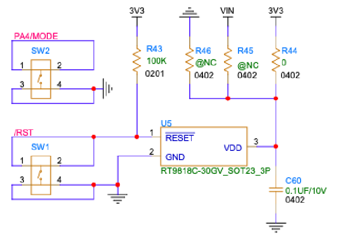
Of note in this design, the VDD pin of the RT9818C is connected to 3V3. The design is configurable by moving a zero-ohm resistor to disable supervisory reset (by connecting to GND) or to use VIN. Note that the RT9818C has a maximum input voltage of 6V which is compatible with the Photon 2. Keep this in mind if using VIN on designs that have larger VIN voltages.
Of course you can simply wire VDD to 3V3 instead of including the configurable resistors.
5V Tolerance
GPIO and all ports such as I2C, SPI, UART serial, etc. are not 5V tolerant. The only pins that are 5V tolerant are:
| Pin | Pin Name | Description | MCU |
|---|---|---|---|
| 12 | VBAT_MEAS | Battery voltage measurement (optional). | |
| 61 | USBDATA+ | USB Data+ | PA[26] |
| 62 | USBDATA- | USB Data- | PA[25] |
BLE (Bluetooth LE)
BLE Central Mode on the P2 and Photon 2 is only supported in Device OS 5.1.0 and later. Earlier versions only supported BLE Peripheral Mode.
Sleep
The P2 can wake from STOP or ULTRA_LOW_POWER sleep mode on any GPIO, RISING, FALLING, or CHANGE.
The P2 can only wake from HIBERNATE sleep mode on pin certain pains, RISING, FALLING, or CHANGE. Pin D10 is the same module pin location (pin 30) as the P1 WKP (A7) pin.
The P2 preserves the state of outputs during STOP or ULTRA_LOW_POWER sleep mode. In HIBERNATE, outputs are high-impedance.
Most pins can use INPUT_PULLUP or INPUT_PULLDOWN in sleep modes. The exceptions in HIBERNATE sleep mode where pins S4, S5, and S6 can only use an external hardware pull-up or pull down.
These P2 pins can wake from HIBERNATE sleep mode:
| Pin | Pin Name | Description | Interface | MCU |
|---|---|---|---|---|
| 30 | D10 / WKP | D10 GPIO, Serial 3 CTS, WKP. (Was WKP/A7 on P1.) | Pin can wake from HIBERNATE sleep | PA[15] |
| 40 | S0 / D15 | S0 GPIO, PWM, SPI MOSI, Serial3 TX, I2S MCLK. (Was P1S0 on P1.) | Pin can wake from HIBERNATE sleep | PA[12] |
| 41 | S1 / D16 | S1 GPIO, PWM, SPI MISO, Serial3 RX. (Was P1S1 on P1.) | Pin can wake from HIBERNATE sleep | PA[13] |
| 42 | S2 / D17 | S2 GPIO, SPI SCK, Serial3 RTS. (Was P1S2 on P1.) | Pin can wake from HIBERNATE sleep | PA[14] |
| 45 | D2 | D2 GPIO, Serial2 RTS, SPI1 MOSI | Pin can wake from HIBERNATE sleep | PA[16] |
| 51 | D3 | D3 GPIO, Serial2 CTS, SPI1 MISO | Pin can wake from HIBERNATE sleep | PA[17] |
| 52 | D4 | D4 GPIO, Serial2 TX, SPI1 SCK | Pin can wake from HIBERNATE sleep | PA[18] |
| 53 | D5 | D5 GPIO, Serial2 RX, SPI1 SS | Pin can wake from HIBERNATE sleep | PA[19] |
These P2 pins have special restrictions on using internal pull-up or pull-down while in HIBERNATE sleep mode. These
also cannot be used as wake from hibernate sleep pins.
| Pin | Pin Name | Description | Interface | MCU |
|---|---|---|---|---|
| 33 | S6 / D21 | S6 GPIO, I2S WS. (Was P1S6/TESTMODE on P1.) | No internal pull up or pull down in HIBERNATE sleep mode. | PB[31] |
| 47 | S4 / D19 | S4 GPIO, I2S RX. (Was P1S4 on P1.) | No internal pull up or pull down in HIBERNATE sleep mode. | PA[0] |
RAM
The P2 has 512 KB of static RAM (SRAM) and 4 MB of pseudo-static RAM (PSRAM).
Around 3072 KB (3 MB) of RAM is available for user applications. Heap allocations are made first from SRAM, then from PSRAM, as necessary.
Retained memory
The P2 and Photon 2 have limited support for retained memory in Device OS 5.3.1 and later:
Retained memory is preserved on RTL872x devices in the following cases:
| Case | Saved |
|---|---|
| When entering sleep modes | 5.3.1 and later |
| OTA firmware updates | 5.3.1 and later |
System.backupRamSync() |
5.3.1 and later |
System.reset() |
Not saved |
| Reset button or reset pin | Not saved |
| Every 10 seconds | 5.3.1 to 5.8.0 only |
Calling System.backupRamSync() will manually save the contents of retained memory to a dedicated flash page on the RTL872x processor and will be restored after the device is reset. You should avoid saving the data extremely frequently as it is slower than RAM and will cause flash wear and is relatively slow to execute.
Prior to Device OS 5.3.1, retained memory is not supported on RTL872x devices. The flash file system can be used, or you can use an external chip such as an I2C or SPI FRAM.
Retained memory is 3068 bytes.
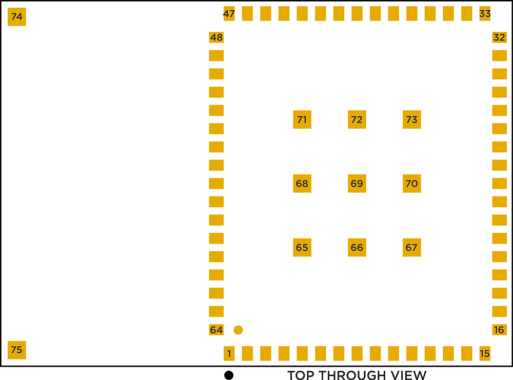
Complete module pin listing

| Pin | Pin Name | Description | MCU |
|---|---|---|---|
| 1 | GND | Ground. Be sure you connect all P1 ground pins. | |
| 2 | 3V3_RF | 3.3V power to RF module | |
| 3 | 3V3_RF | 3.3V power to RF module | |
| 4 | GND | Ground. Be sure you connect all P1 ground pins. | |
| 5 | 3V3_IO | 3.3V power to MCU IO. | |
| 6 | GND | Ground. Be sure you connect all P1 ground pins. | |
| 7 | NC | No connection. Do not connect anything to this pin. | |
| 8 | NC | No connection. Do not connect anything to this pin. | |
| 9 | NC | No connection. Do not connect anything to this pin. | |
| 10 | NC | No connection. Do not connect anything to this pin. | |
| 11 | NC | No connection. Do not connect anything to this pin. | |
| 12 | VBAT_MEAS | Battery voltage measurement (optional). | |
| 13 | GND | Ground. Be sure you connect all P1 ground pins. | |
| 14 | NC | No connection. Do not connect anything to this pin. | |
| 15 | GND | Ground. Be sure you connect all P1 ground pins. | |
| 16 | NC | No connection. Do not connect anything to this pin. | |
| 17 | NC | No connection. Do not connect anything to this pin. | |
| 18 | NC | No connection. Do not connect anything to this pin. | |
| 19 | NC | No connection. Do not connect anything to this pin. | |
| 20 | NC | No connection. Do not connect anything to this pin. | |
| 21 | NC | No connection. Do not connect anything to this pin. | |
| 22 | NC | No connection. Do not connect anything to this pin. | |
| 23 | A5 / D14 | A5 Analog in, GPIO, PWM. | PB[4] |
| 24 | NC | No connection. Do not connect anything to this pin. | |
| 25 | GND | Ground. Be sure you connect all P1 ground pins. | |
| 26 | 3V3 | 3.3V power to MCU | |
| 27 | 3V3 | 3.3V power to MCU | |
| 28 | GND | Ground. Be sure you connect all P1 ground pins. | |
| 29 | RGBR | RGB LED Red. Has 10K hardware pull-up. Do not hold low at boot. | PA[30] |
| 30 | D10 / WKP | D10 GPIO, Serial 3 CTS, WKP. (Was WKP/A7 on P1.) | PA[15] |
| 31 | RGBB | RGB LED Blue | PB[22] |
| 32 | RGBG | RGB LED Green | PB[23] |
| 33 | S6 / D21 | S6 GPIO, I2S WS. (Was P1S6/TESTMODE on P1.) | PB[31] |
| 34 | RST | Hardware reset. Pull low to reset; can leave unconnected in normal operation. | CHIP_EN |
| 35 | D1 / A4 | D1 GPIO, PWM, I2C SCL, A4 Analog In | PB[5] |
| 36 | D0 / A3 | D0 GPIO, I2C SDA, A3 Analog In | PB[6] |
| 37 | GND | Ground. Be sure you connect all P1 ground pins. | |
| 38 | NC | No connection. Do not connect anything to this pin. | |
| 39 | GND | Ground. Be sure you connect all P1 ground pins. | |
| 40 | S0 / D15 | S0 GPIO, PWM, SPI MOSI, Serial3 TX, I2S MCLK. (Was P1S0 on P1.) | PA[12] |
| 41 | S1 / D16 | S1 GPIO, PWM, SPI MISO, Serial3 RX. (Was P1S1 on P1.) | PA[13] |
| 42 | S2 / D17 | S2 GPIO, SPI SCK, Serial3 RTS. (Was P1S2 on P1.) | PA[14] |
| 43 | A1 / D12 | A1 Analog in, PDM DAT, GPIO | PB[2] |
| 44 | S3 / D18 | S3 GPIO, I2S TX. (Was P1S3 on P1.), SPI SS | PB[26] |
| 45 | D2 | D2 GPIO, Serial2 RTS, SPI1 MOSI | PA[16] |
| 46 | MODE | MODE button. Pin number constant is BTN. External pull-up required! | PA[4] |
| 47 | S4 / D19 | S4 GPIO, I2S RX. (Was P1S4 on P1.) | PA[0] |
| 48 | S5 / D20 | S5 GPIO, I2S CLK. (Was P1S5 on P1.) | PB[29] |
| 49 | A2 / D13 | A2 Analog in, PWM, GPIO | PB[7] |
| 50 | A0 / D11 | A0 Analog in, PDM CLK, GPIO | PB[1] |
| 51 | D3 | D3 GPIO, Serial2 CTS, SPI1 MISO | PA[17] |
| 52 | D4 | D4 GPIO, Serial2 TX, SPI1 SCK | PA[18] |
| 53 | D5 | D5 GPIO, Serial2 RX, SPI1 SS | PA[19] |
| 54 | D7 | D7 GPIO, SWDIO | PA[27] |
| 55 | D6 | D6 GPIO, SWCLK | PB[3] |
| 56 | NC | No connection. Do not connect anything to this pin. | |
| 57 | NC | No connection. Do not connect anything to this pin. | |
| 58 | NC | No connection. Do not connect anything to this pin. | |
| 59 | GND | Ground. Be sure you connect all P1 ground pins. | |
| 60 | NC | No connection. Do not connect anything to this pin. | |
| 61 | USBDATA+ | USB Data+ | PA[26] |
| 62 | USBDATA- | USB Data- | PA[25] |
| 63 | RX / D9 | Serial1 RX (received data), GPIO | PA[8] |
| 64 | TX / D8 | Serial1 TX (transmitted data), GPIO | PA[7] |
| 65 | GND | Ground. Be sure you connect all P1 ground pins. | |
| 66 | GND | Ground. Be sure you connect all P1 ground pins. | |
| 67 | GND | Ground. Be sure you connect all P1 ground pins. | |
| 68 | GND | Ground. Be sure you connect all P1 ground pins. | |
| 69 | GND | Ground. Be sure you connect all P1 ground pins. | |
| 70 | GND | Ground. Be sure you connect all P1 ground pins. | |
| 71 | GND | Ground. Be sure you connect all P1 ground pins. | |
| 72 | GND | Ground. Be sure you connect all P1 ground pins. | |
| 73 | GND | Ground. Be sure you connect all P1 ground pins. | |
| 74 | NC | No connection. Do not connect anything to this pin. | |
| 75 | NC | No connection. Do not connect anything to this pin. |
Complete module pin details


Technical specification
Recommended operating conditions
| Parameter | Symbol | Min | Typ | Max | Unit |
|---|---|---|---|---|---|
| Operating Temperature | Top | -20 | +70 | °C | |
| Humidity Range Non condensing, relative humidity | 95 | % |
I/O Characteristics
| Parameter | Symbol | Min | Typ | Peak | Unit |
|---|---|---|---|---|---|
| Input-High Voltage | VIH | 2.0 | V | ||
| Input-Low Voltage | VIL | 0.8 | V | ||
| Output drive strength (normal drive) | 4 | mA | |||
| Output drive strength (high drive) | 12 | mA | |||
| Total output drive (all pins) | 200 | mA |
Power consumption
| Parameter | Symbol | Min | Typ | Peak | Unit |
|---|---|---|---|---|---|
| Operating Current (uC on, peripherals and radio disabled) | Iidle | 63.8 | 65.8 | 68.9 | mA |
| Operating Current (uC on, BLE advertising) | Ible_adv | 62.4 | 66.1 | 73.8 | mA |
| Operating Current (uC on, radio connected to access point) | Iwifi_conn_ap | 62.3 | 67.8 | 325 | mA |
| STOP mode sleep, GPIO wake-up | Istop_gpio | 549 | 579 | 608 | uA |
| STOP mode sleep, time wake-up | Istop_intrtc | 543 | 572 | 604 | uA |
| ULP mode sleep, GPIO wake-up | Iulp_gpio | 549 | 579 | 608 | uA |
| ULP mode sleep, time wake-up | Iulp_intrtc | 543 | 572 | 604 | uA |
| HIBERNATE mode sleep, GPIO wake-up | Ihib_gpio | 93.8 | 114 | 133 | uA |
| HIBERNATE mode sleep, time wake-up | Ihib_intrtc | 93.3 | 115 | 133 | uA |
1The min, and particularly peak, values may consist of very short transients. The typical (typ) values are the best indicator of overall power consumption over time. The peak values indicate the absolute minimum capacity of the power supply necessary, not overall consumption.
Mechanical specifications
Module dimensions
- P2 module dimensions are: 0.787"(28mm) (W) x 1.102"(20mm) (L) x 0.118"(3.0mm) (H) +/-0.0039"(0.1mm) (includes metal shielding)
Recommended PCB land pattern
The P2 can be mounted directly on a carrier PCB with following PCB land pattern:
A P1/P2 part for EAGLE can be found in the Particle EAGLE library.
When laying out your board:
- The area in the component keep-out (1) must be free of ground plane, traces, and components on the top or bottom of the board. This will be enforced by Eagle CAD.
- Avoid having a strip of ground plane next to the antenna (2). This is easy to do accidentally, and should be avoided.
- When possible, avoid ground plane in area (3). If you need to put traces or components in this area, it can be done if there is no convenient alternative, but it's best to keep the area close to the antenna as empty as possible for best RF performance.
3D models
3D models of the P2 module are available in the hardware-libraries Github in formats including step, iges, and f3z.
Reference design
A P2 reference design is available in Github. The repository includes schematics, board layout, footprints, for Eagle CAD.
Recommended solder reflow profile
[This information is from the P1, and is likely to remain the same, but is subject to change.]
| Phase | Temperatures and Rates |
|---|---|
| A-B. | Ambient - 150°C, Heating rate: < 3°C/s |
| B-C. | 150 - 200°C, soak time: 60 - 120 s |
| C-D. | 200 - 245°C, Heating rate: < 3°C/s |
| D. | Peak temp.: 235 - 245°C, Time above 220°C: 40 - 90 s |
| D-E. | 245 - 220°C, Cooling rate: < 1°C/s |
Ordering information
P2 modules are available from store.particle.io as cut tape in quantities of 10 each.
| SKU | Description | Region | Lifecycle | Replacement |
|---|---|---|---|---|
| P2MOD10 | P2 Wi-Fi Module, Cut tape [x10] | Global | GA | |
| P2REEL | P2 Wi-Fi Module, Reel [x600] | Global | GA |
Qualification and approvals

- RoHS
- CE
- FCC ID: 2AEMI-P2
- ISED: 20127-P2
Product handling
Moisture sensitivity levels
The Moisture Sensitivity Level (MSL) relates to the packaging and handling precautions required. The P1 module is rated level 3. In general, this precaution applies for Photons without headers. When reflowing a P1 directly onto an application PCB, increased moisture levels prior to reflow can damage sensitive electronics on the P1. A bake process to reduce moisture may be required.
For more information regarding moisture sensitivity levels, labeling, storage and drying see the MSL standard see IPC/JEDEC J-STD-020 (can be downloaded from www.jedec.org).
ESD precautions
The P1 module contains highly sensitive electronic circuitry and is an Electrostatic Sensitive Device (ESD). Handling a P1 module without proper ESD protection may destroy or damage it permanently. Proper ESD handling and packaging procedures must be applied throughout the processing, handling and operation of any application that incorporates P1 modules. ESD precautions should be implemented on the application board where the P1 module is mounted. Failure to observe these precautions can result in severe damage to the P1 module!
Assembly
Water soluble flux
Water soluble flux should not be used with the P2 module. There are components within the module that are moisture-sensitive, and wash water can get trapped under the RF shields, causing damage.
Use no-clean flux instead.
Conformal coatings
We do not recommend using a conformal coating on the P2 module to protect the module from water. Some components on the module cannot be coated and would need to be masked off during coating. This will make the coating process difficult to implement and test.
Using an enclosure that protects both your base board and the P2 module as a single waterproof assembly is recommended instead.
Default settings
The P2 module comes pre-programmed with a bootloader and a user application called Tinker. This application works with an iOS and Android app also named Tinker that allows you to very easily toggle digital pins, take analog and digital readings and drive variable PWM outputs.
The bootloader allows you to easily update the user application via several different methods, USB, OTA, Serial Y-Modem, and also internally via the Factory Reset procedure. All of these methods have multiple tools associated with them as well.
You may use the Particle Web IDE to code, compile and flash a user application OTA (Over The Air). Particle Workbench is a full-featured desktop IDE for Windows, Mac, and Linux based on VSCode and supports both cloud-based and local gcc-arm compiles. The Particle CLI provides a command-line interface for cloud-based compiles and flashing code over USB.
Intended applications
The P2 module is intended to be used for Wi-Fi based Internet-of-Things (IoT) applications such as environment, weather, HVAC, equipment, and security monitoring.
The P2 is not certified for use as a wearable device.
Glossary
FCC ISED CE warnings and end product labeling requirements
The FCC, ISED, and CE certifications are radio module certifications only. Additional certification will be required for your completed system.
United States (FCC)
Federal Communication Commission Interference Statement This equipment has been tested and found to comply with the limits for a Class B digital device, pursuant to Part 15 of the FCC Rules. These limits are designed to provide reasonable protection against harmful interference in a residential installation. This equipment generates, uses and can radiate radio frequency energy and, if not installed and used in accordance with the instructions, may cause harmful interference to radio communications. However, there is no guarantee that interference will not occur in a particular installation. If this equipment does cause harmful interference to radio or television reception, which can be determined by turning the equipment off and on, the user is encouraged to try to correct the interference by one of the following measures:
- Reorient or relocate the receiving antenna.
- Increase the separation between the equipment and receiver.
- Connect the equipment into an outlet on a circuit different from that to which the receiver is connected.
- Consult the dealer or an experienced radio/TV technician for help.
FCC Caution: Any changes or modifications not expressly approved by the party responsible for compliance could void the user's authority to operate this equipment. This device complies with Part 15 of the FCC Rules. Operation is subject to the following two conditions:
- This device may not cause harmful interference, and
- This device must accept any interference received, including interference that may cause undesired operation.
FCC Radiation Exposure Statement: This equipment complies with FCC radiation exposure limits set forth for an uncontrolled environment. This transmitter module must not be co-located or operating in conjunction with any other antenna or transmitter. This End equipment should be installed and operated with a minimum distance of 20 centimeters between the radiator and your body.
IMPORTANT NOTE: In the event that these conditions can not be met (for example certain laptop configurations or co-location with another transmitter), then the FCC authorization is no longer considered valid and the FCC ID can not be used on the final product. In these circumstances, the OEM integrator will be responsible for re-evaluating the end product (including the transmitter) and obtaining a separate FCC authorization.
End Product Labeling The final end product must be labeled in a visible area with the following:
Contains FCC ID: 2AEMI-P2
Manual Information to the End User The OEM integrator has to be aware not to provide information to the end user regarding how to install or remove this RF module in the user’s manual of the end product which integrates this module.
Outdoor Use (US)
To be compliant to FCC §15.407(a) the EIRP is not allowed to exceed 125 mW (21 dBm) at any elevation angle above 30° (measured from the horizon) when operated as an outdoor access point in U-NII-1 band, 5.150-5.250 GHz.
Canada (ISED)
Canada Statement This device complies with Industry Canada’s licence-exempt RSSs. Operation is subject to the following two conditions:
- This device may not cause interference; and
- This device must accept any interference, including interference that may cause undesired operation of the device.
Le présent appareil est conforme aux CNR d’Industrie Canada applicables aux appareils radio exempts de licence.
L’exploitation est autorisée aux deux conditions suivantes:
- l’appareil ne doit pas produire de brouillage;
- l’utilisateur de l’appareil doit accepter tout brouillage radioélectrique subi, même si le brouillage est susceptible d’en compromettre le fonctionnement.
Caution Exposure: This device meets the exemption from the routine evaluation limits in section 2.5 of RSS102 and users can obtain Canadian information on RF exposure and compliance. Le dispositif répond à l'exemption des limites d'évaluation de routine dans la section 2.5 de RSS102 et les utilisateurs peuvent obtenir des renseignements canadiens sur l'exposition aux RF et le respect.
The final end product must be labelled in a visible area with the following: The Industry Canada certification label of a module shall be clearly visible at all times when installed in the host device, otherwise the host device must be labelled to display the Industry Canada certification number of the module, preceded by the words “Contains transmitter module”, or the word “Contains”, or similar wording expressing the same meaning, as follows:
Contains transmitter module ISED: 20127-P2
This End equipment should be installed and operated with a minimum distance of 20 centimeters between the radiator and your body. Cet équipement devrait être installé et actionné avec une distance minimum de 20 centimètres entre le radiateur et votre corps.
The end user manual shall include all required regulatory information/warning as shown in this manual.
Outdoor use (CA)
- Operation in the band 5150–5250 MHz is only for indoor use to reduce the potential for harmful interference to co-channel mobile satellite systems;
- Operation in the 5600-5650 MHz band is not allowed in Canada. High-power radars are allocated as primary users (i.e., priority users) of the bands 5250-5350 MHz and 5650-5850 MHz and that these radars could cause interference and/or damage to LE-LAN devices.
- Le dispositif de fonctionnement dans la bande 5150-5250 MHz est réservé à une utilisation en intérieur pour réduire le risque d'interférences nuisibles à la co-canal systèmes mobiles par satellite
- Opération dans la bande 5600-5650 MHz n'est pas autorisée au Canada. Haute puissance radars sont désignés comme utilisateurs principaux (c.-àutilisateurs prioritaires) des bandes 5250-5350 MHz et 5650-5850 MHz et que ces radars pourraient causer des interférences et / ou des dommages à dispositifs LAN-EL.
European Union (CE)
We, Particle Industries,Inc, declare under our sole responsibility that the product, P2, to which this declaration relates, is in conformity with RED Directive 2014/53/EU and (EU) 2015/863 RoHS Directive 2011/65/EU (Recast).
The full text of the EU declaration of conformity is available at the followingInternet address: https://www.particle.io/
Radiation Exposure Statement: This equipment complies with radiation exposure limits set forth for an uncontrolled environment.
The operating frequency bands and the maximum transmitted power limit are listed below:
- BLE 2402-2480MHz 10dBm
- Wi-Fi 2.4GHz band 2412-2484MHz 20dBm
- Wi-Fi 5GHz band 5180-5825MHz 23dBm
United Kingdom
UKCA Conformity:
Radio Equipment Regulations 2017 (S.I. 2017/1206)
Outdoor use (world)
This device is restricted to indoor use when operating in the 5150 to 5350 MHz frequency range. This restriction applies in: AT, BE, BG, CH, CY, CZ, DE, DK, EE, EL, ES, FI, FR, HR, HU, IE, IS, IT, LI, LT, LU, LV, MT, NL, NO, PL, PT, RO, SE, SI, SK, TR, UA, UK(NI).
Certification documents
Bluetooth - P2
CE (Europe) - P2
- EU Declaration of Conformity (updated 2026-05-18)
- Certificate of Conformity
- EN 300-328 Bluetooth LE Test Report
- EN 300-328 Wi-Fi Test Report
- EN 300-440 Wi-Fi 5 GHz Test Report
- EN 301-489 Test Report
- EN 301-893 Wi-Fi 5 GHz Test Report
- EN 301-893 Dynamic Frequency Selection DFS Test Report
- EN62311 Test Report
- EN62368 Test Report
- EN62479 Test Report
FCC (United States) - P2
- FCC ID: 2AEMI-P2
- FCC Grant of Equipment Authorization (DTS)
- FCC Grant of Equipment Authorization (NII)
- RF Exposure Report FCC Part 2, Section 2.1091
- FCC 15.247 Bluetooth LE Test Report
- FCC 15.247 Wi-Fi Test Report
- FCC 15.407 Test Report
- FCC 15.407 Test Report (5 GHz Wi-Fi)
ISED (Canada) - P2
- ISED: 20127-P2
- Certificate of Conformity
- ISED RSS-247 BTLE Test Report
- ISED RSS-247 Wi-Fi 2.4 GHz Test Report
- ISED RSS-247 Wi-Fi 5 GHz Test Report
- ISED RSS-247 DFS Test Report;
- ISED RSS-102 RF Exposure Report
RoHS - P2
UKCA (United Kingdom) - P2
Trace antenna test report - P2
Revision history
| Revision | Date | Author | Comments |
|---|---|---|---|
| pre | 2021-11-04 | RK | Pre-release |
| 2022-02-08 | RK | Corrected D pin aliases for A5 and S0-S6 | |
| 2022-02-25 | RK | Changed D pin aliases for D9 - D22, A5 is not SPI MOSI, Serial2 TX and RX were reversed | |
| 2022-03-14 | RK | Minor edits; no functional changes | |
| 2022-03-23 | RK | Added FCC and ISED IDs, operating temperature range | |
| 2022-04-12 | RK | Added serial baud rates | |
| 2022-04-16 | RK | Added Serial3 | |
| 2022-05-07 | RK | Temperature range is -20°C to +70°C | |
| 2022-05-27 | RK | Updated antenna information, rendering | |
| 2022-06-03 | RK | Added note about module certification | |
| 2022-06-08 | RK | Added intended applications section, changed reference to ARM M4F to M33 | |
| 2022-06-29 | RK | Added flash memory map | |
| 2022-07-14 | RK | No hardware pull-up on MODE pin | |
| 2022-07-22 | RK | Added power consumption | |
| 2022-08-12 | RK | Added listing of pins used at boot | |
| 2022-08-12 | RK | Warning about BLE central mode not available | |
| 2022-08-18 | RK | EU certification statement | |
| 2022-09-16 | RK | Added UKCA conformity | |
| 2022-11-08 | RK | Added external antenna | |
| 2022-11-16 | RK | Added additional board layout tips | |
| 2022-11-17 | RK | Pin D0 does not have PWM | |
| 2022-12-16 | RK | Added warning about using RGBR as GPIO because of the 10K pull-up | |
| 2023-01-31 | RK | Add Device OS versions | |
| 001 | 2023-03-08 | RK | Main CPU (KM4) is M33, not M23 |
| 002 | 2023-03-14 | RK | Added power supply specifications |
| 003 | 2023-04-05 | RK | Added Device OS 5.3.1 information for SPI and retained memory |
| 004 | 2023-04-10 | RK | Outdoor use restrictions |
| 005 | 2023-04-24 | RK | Document VBAT_MEAS |
| 006 | 2023-04-28 | RK | Add conformal coating and flux notes |
| 007 | 2023-05-05 | RK | Update available RAM |
| 008 | 2023-05-11 | RK | Add link to reference design |
| 009 | 2023-06-07 | RK | Add module height (3mm) |
| 010 | 2023-07-07 | RK | Add supervisory reset IC recommendation |
| 011 | 2023-09-08 | RK | Add 5V tolerance section |
| 012 | 2023-11-13 | RK | Add full pin details |
| 013 | 2023-12-20 | RK | Add boot mode pin information to GPIO pin listing |
| 014 | 2024-02-20 | RK | Added pin drive strength |
| 015 | 2024-03-11 | RK | Added boot mode pin warning to GPIO pin table |
| 016 | 2024-04-18 | RK | Add PDM microphone |
| 017 | 2024-04-23 | RK | Added links to certification documents |
| 018 | 2024-04-25 | RK | Update retained memory description |
| 019 | 2024-04-25 | RK | Added I/O characteristics |
| 020 | 2024-08-21 | RK | Added supervisory reset information |
| 021 | 2024-09-04 | RK | Added note about VBAT_MEAS |
| 022 | 2024-10-02 | RK | Added warning to not use Argon (ANT-FLXV2) antenna |
| 023 | 2026-05-18 | RK | Updated EU Declaration of Conformity |
Known errata
Contact
Web
https://www.particle.io
Community Forums
https://community.particle.io