System integration manual
This manual provides the necessary guidelines to successfully integrate the E series module in your product.
For further information about this module please refer to:
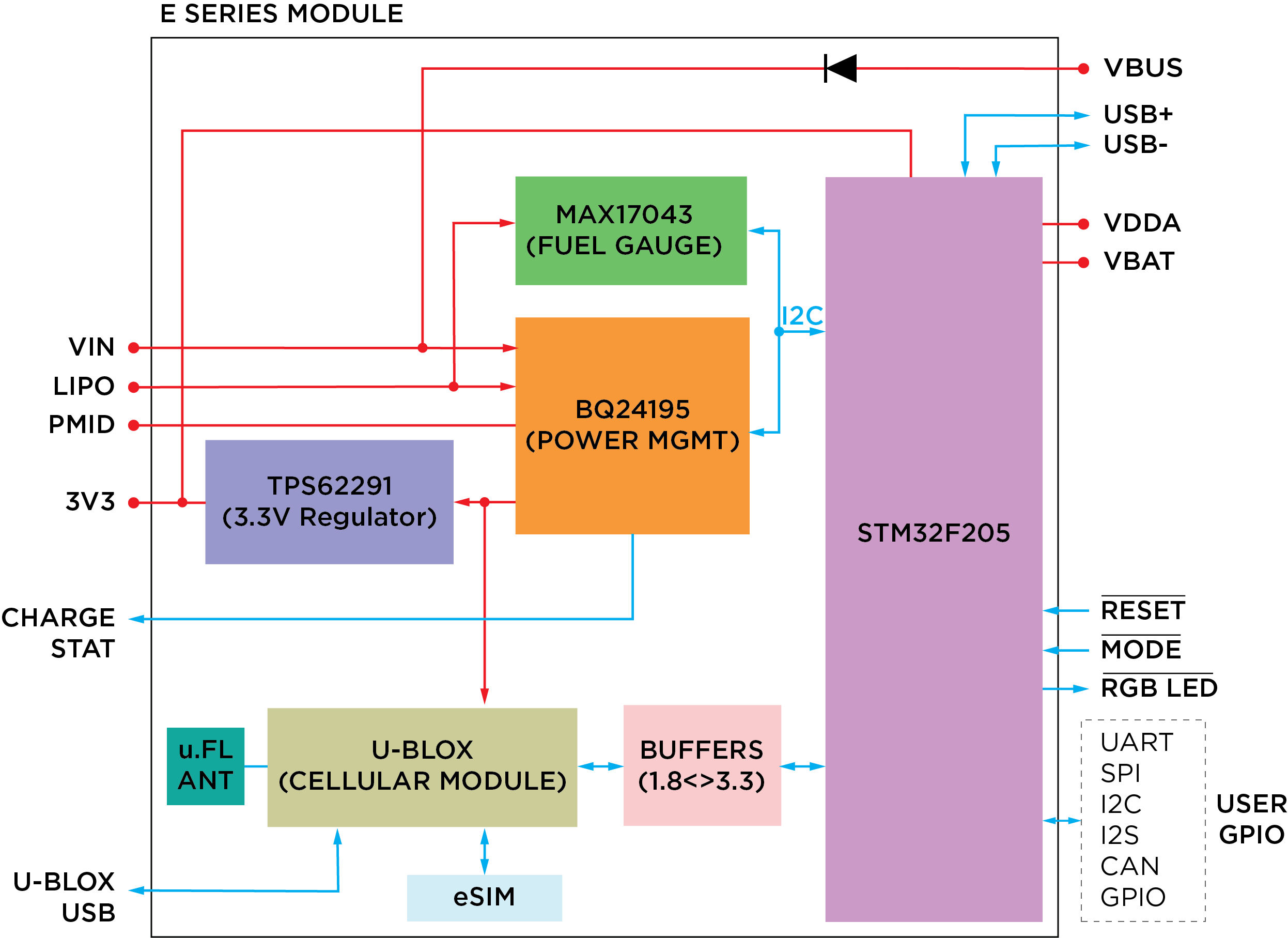
E-Series architecture:
The block diagram below summarizes the architecture of the E series module. It's key components are the STM32F205 microcontroller and the u-blox SARA cellular modem. In addition to that, the module has an on board power management IC, 3.3V DC regulator, LiPo fuel gauge, and an Particle embedded SIM chip. There is also room for additional SPI based FLASH memory expansion.
Overview
Pinout diagram

You can download a high resolution pinout diagram in a PDF version here.
Pin description
| # | PIN | FUNCTION | DESCRIPTION |
|---|---|---|---|
| 1 | VIN | POWER | This pin can be used as an input or output. As an input, supply 5VDC to 12VDC to power the Electron. When the Electron is powered via the USB port, this pin will output a voltage of approximately 4.8VDC due to a reverse polarity protection series Schottky diode between VBUS and VIN. When used as an output, the max load on VIN is 1Amp. |
| 2 | GND | POWER | System ground. |
| 3 | VBUS | POWER | This is connected to the VBUS power pin of the USB port. |
| 4 | GND | POWER | System ground. |
| 5 | LiPo | POWER | This is connected to the +LiPo connector. |
| 6 | NC | TBD | Do not connect. |
| 7 | GND | POWER | System ground. |
| 8 | PMID | POWER | This is connected to the PMID pin of the PMIC. |
| 9 | 3V3 | POWER | This is the output of the 3V3 regulator on the E0. |
| 10 | VDDA | POWER | This is the input to the analog block of the STM32. |
| 11 | VBAT | POWER | Supply to the internal RTC, backup registers and SRAM when 3V3 is not present (1.65 to 3.6VDC). |
| 12 | GND | POWER | System ground. |
| 13 | USB+ | IO | Data+ pin of the USB port. |
| 14 | USB- | IO | Data- pin of the USB port. |
| 15 | GND | POWER | System ground. |
| 16 | TX | IO | Primarily used as UART TX, but can also be used as a digital GPIO or PWM. |
| 17 | RX | IO | Primarily used as UART RX, but can also be used as a digital GPIO or PWM. |
| 18 | GND | POWER | System ground. |
| 19 | WKP | IO | Active-high wakeup pin, wakes the module from sleep/standby modes. When not used as a WAKEUP, this pin can also be used as a digital GPIO, ADC input or PWM. Can be referred to as A7 when used as an ADC. |
| 20 | DAC | IO | 12-bit Digital-to-Analog (D/A) output (0-4095), referred to as DAC or DAC1 in software. Can also be used as a digital GPIO or ADC. Can be referred to as A6 when used as an ADC. |
| 21 | A5 | IO | 12-bit Analog-to-Digital (A/D) inputs (0-4095), and also digital GPIOs. |
| 22 | A4 | IO | 12-bit Analog-to-Digital (A/D) inputs (0-4095), and also digital GPIOs. |
| 23 | A3 | IO | 12-bit Analog-to-Digital (A/D) inputs (0-4095), and also digital GPIOs. |
| 24 | A2 | IO | 12-bit Analog-to-Digital (A/D) inputs (0-4095), and also digital GPIOs. |
| 25 | A1 | IO | 12-bit Analog-to-Digital (A/D) inputs (0-4095), and also digital GPIOs. |
| 26 | A0 | IO | 12-bit Analog-to-Digital (A/D) inputs (0-4095), and also digital GPIOs. |
| 27 | GND | POWER | System ground. |
| 28 | B5 | IO | 12-bit Analog-to-Digital (A/D) inputs (0-4095), and also digital GPIOs. |
| 29 | B4 | IO | 12-bit Analog-to-Digital (A/D) inputs (0-4095), and also digital GPIOs. |
| 30 | B3 | IO | 12-bit Analog-to-Digital (A/D) inputs (0-4095), PWM and also digital GPIOs. |
| 31 | B2 | IO | 12-bit Analog-to-Digital (A/D) inputs (0-4095), PWM and also digital GPIOs. |
| 32 | B1 | IO | Digital only GPIO, and PWM. |
| 33 | B0 | IO | Digital only GPIO, and PWM. |
| 34 | GND | POWER | System ground. |
| 35 | D7 | IO | Digital only GPIO. |
| 36 | D6 | IO | Digital only GPIO. |
| 37 | D5 | IO | Digital only GPIO. |
| 38 | D4 | IO | Digital only GPIO. |
| 39 | D3 | IO | Digital only GPIO, and PWM. |
| 40 | D2 | IO | Digital only GPIO, and PWM. |
| 41 | D1 | IO | Digital only GPIO, and PWM. |
| 42 | D0 | IO | Digital only GPIO, and PWM. |
| 43 | GND | POWER | System ground. |
| 44 | C5 | IO | Digital only GPIO, and PWM. |
| 45 | C4 | IO | Digital only GPIO, and PWM. |
| 46 | C3 | IO | Digital only GPIO. |
| 47 | C2 | IO | Digital only GPIO. |
| 48 | C1 | IO | Digital only GPIO. |
| 49 | C0 | IO | Digital only GPIO. |
| 50 | NC | TBD | Do not connect. |
| 51 | GND | POWER | System ground. |
| 52 | BLU | IO | Blue pin of the RGB LED. |
| 53 | GRN | IO | Green pin of the RGB LED. |
| 54 | RED | IO | Red pin of the RGB LED. |
| 55 | MODE | IO | Connected to the MODE button input. |
| 56 | RST | I | Active-low reset input. |
| 57 | STAT | O | Connected to the charge status pin of the PMIC. |
| 58 | GND | POWER | System ground. |
| 59 | GND | POWER | System ground. |
| 60 | GND | POWER | System ground. |
| 61 | UB_USB+ | IO | Data+ pin of the u-blox USB port. |
| 62 | UB_USB- | IO | Data- pin of the u-blox USB port. |
| 63 | UB_VUSB_DET | IO | USB detect pin of the u-blox USB port. 5V on this pin enables the u-blox's USB interface. |
[1] PWM is available on D0, D1, D2, D3, B0, B1, B2, B3, A4, A5, WKP, RX, TX with a caveat: PWM timer peripheral is duplicated on two pins (A5/D2) and (A4/D3) for 11 total independent PWM outputs. For example: PWM may be used on A5 while D2 is used as a GPIO, or D2 as a PWM while A5 is used as an analog input. However A5 and D2 cannot be used as independently controlled PWM outputs at the same time.
Technical specifications
Absolute maximum ratings [1]
| Parameter | Symbol | Min | Typ | Max | Unit |
|---|---|---|---|---|---|
| Supply Input Voltage | VIN-MAX | +17 | V | ||
| Supply Output Current | IIN-MAX-L | 1 | A | ||
| Battery Input Voltage | VLiPo | +6 | V | ||
| Supply Output Current | I3V3-MAX-L | 800 | mA | ||
| Storage Temperature | Tstg | -30 | +75 | °C | |
| ESD Susceptibility HBM (Human Body Mode) | VESD | 2 | kV |
[1] Stresses beyond those listed under absolute maximum ratings may cause permanent damage to the device. These are stress ratings only, and functional operation of the device at these or any other conditions beyond those indicated under recommended operating conditions is not implied. Exposure to absolute-maximum-rated conditions for extended periods may affect device reliability.
Recommended operating conditions
| Parameter | Symbol | Min | Typ | Max | Unit |
|---|---|---|---|---|---|
| Supply Input Voltage | VIN | +3.88[1] | +12 | V | |
| Supply Output Voltage | VIN | +4.8 | V | ||
| Supply Output Voltage | V3V3 | +3.3 | V | ||
| LiPo Battery Voltage | VLiPo | +3.6 | +4.4 | V | |
| Supply Input Voltage | VVBAT | +1.65 | +3.6 | V | |
| Supply Input Current (VBAT) | IVBAT | 19 | uA | ||
| Operating Current (uC on, Cellular ON) | IIN avg | 180 | 250 | mA | |
| Peak Current (uC on, Cellular ON) | IIN pk | 800[2] | 1800[3] | mA | |
| Operating Current (uC on, Cellular OFF) | IIN avg | 47 | 50 | mA | |
| Sleep Current (4.2V LiPo, Cellular OFF) | IQs | 0.8 | 2 | mA | |
| Deep Sleep Current (4.2V LiPo, Cellular OFF) | IQds | 110 | 130 | uA | |
| Operating Temperature | Top | -20 | +60 | °C | |
| Humidity Range Non condensing, relative humidity | 95 | % |
Notes:
[1] The minimum input voltage is software defined with a user selectable range of 3.88V to 5.08V in 80mV increments. Out of the box, the minimum input voltage is set to 4.36V in order for the LiPo battery to be able to properly charge.
[2] 3G operation
[3] 2G operation
Design
Power supply interface
The E series modules can be powered over VIN, VBUS, LiPo or a combination of them. The VIN and VBUS pins are connected to the input of the power management IC which handles regulation, charging and powering of system. The VIN pin is directly connected to the input while VBUS pin has a reverse polarity protection diode so that power over VIN does not back feed into the USB port. You will see a drop of 0.43 V at the input when powered over USB.
Tip: Most of the power requirements of the E series module are dictated by the u-blox's SARA cellular modem, so it is important that you also refer to the SARA-G3 and SARA-U2-series System Integration Manual's section 1.5.
Powering using a battery:
The E series module uses TI's BQ24195 to do all of its power management. It is designed to charge a single cell Li-Ion or Li-Polymer battery while intelligently switching between charging and discharging based on the presence of an additional power supply. You can power your design with a battery alone or use it as a back up in addition to having a permanent DC source. The two things you need to keep in mind while choosing a battery is its cell chemistry and max discharge rate. The on board PMIC only supports single cell Li Ion and Li Polymer (3.7V) chemistry. The discharge rate should be able equal to or greater that 2A to meet the cellular modems peak current requirements. The battery provided with the E series evaluation kit is rated at 1,800mAH and a discharge rate of 1C with internal over current protection.
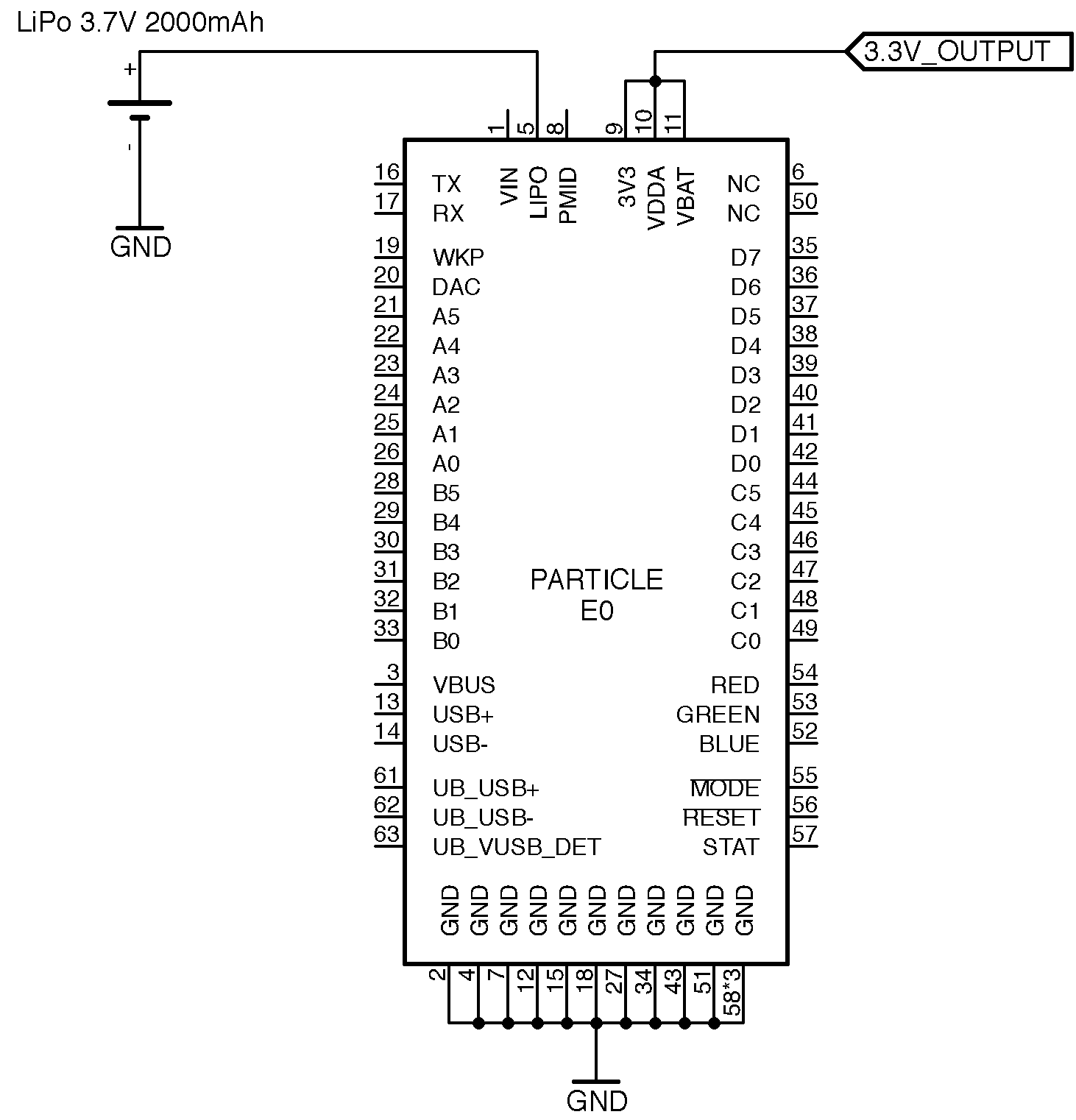
Powering over VIN along with the LiPo battery
If you are planning to use a different cell chemistry or voltage, you'll have to design its charging and management separately.
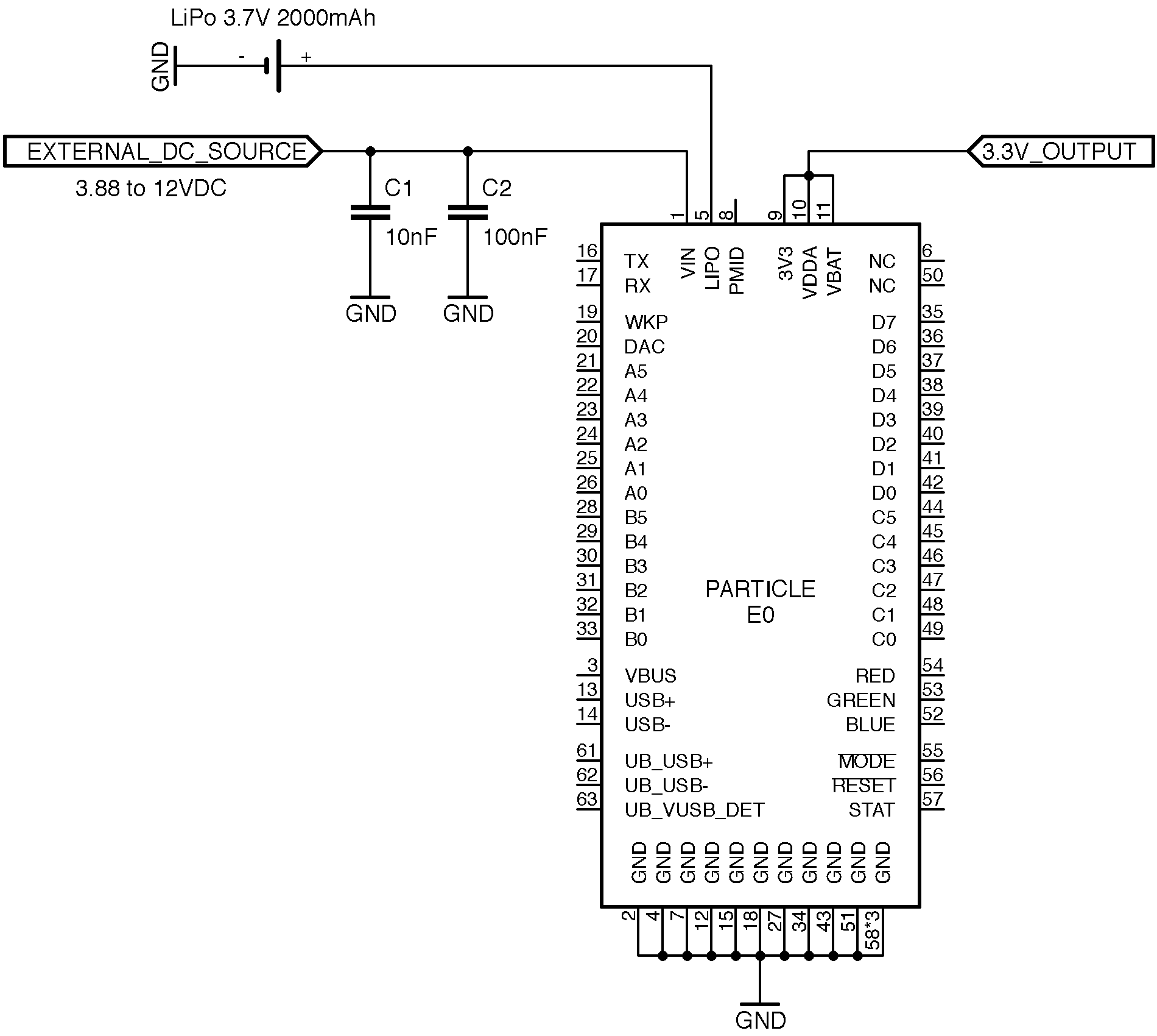
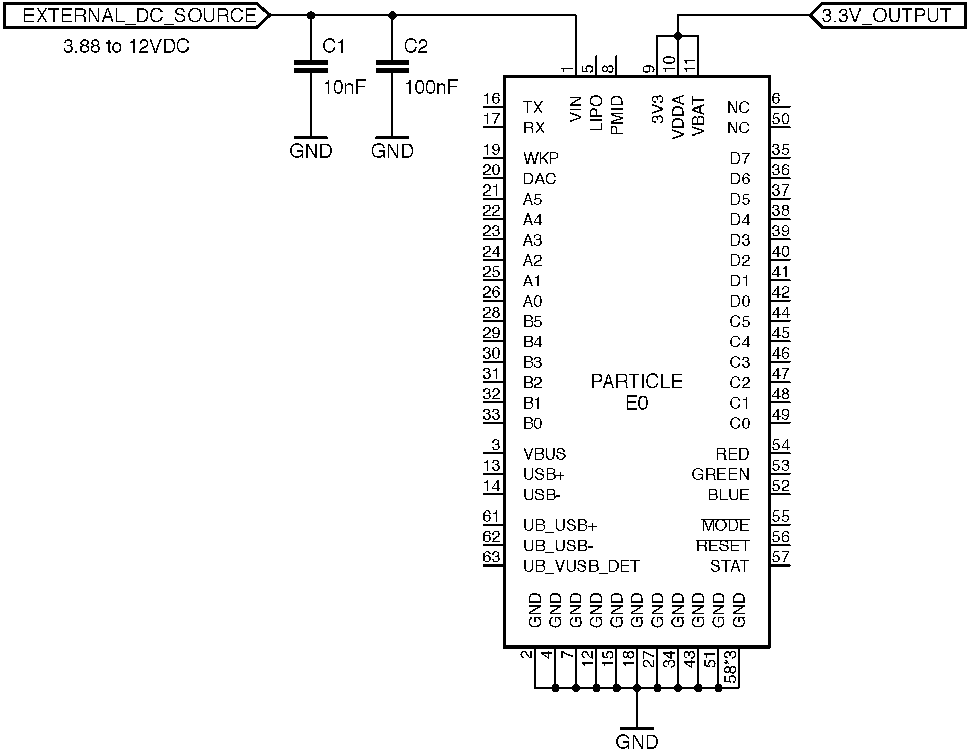
Powering using an external DC source
VIN
The E series module can be powered from an external DC source via the VIN pin. The pin can accept voltages from 3.88V to 12VDC. For continuous operation without a battery, please spec the power supply at 10 Watts. For example, if powering at 5 V, the supply should be able to supply 2 A of current.
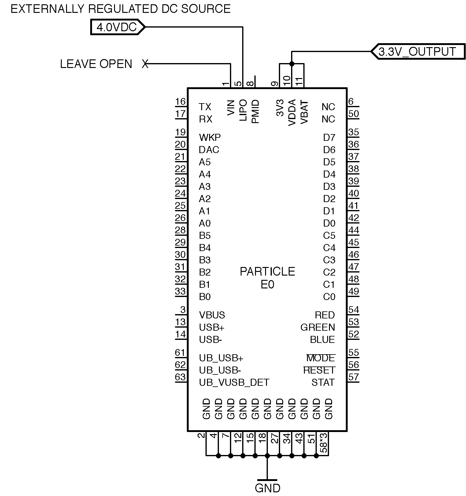
LiPo
You can also bypass the PMIC's internal regulator and power the module directly by connecting an externally regulated DC source (3.8 V to 4.1 V) to the LiPo pin as long as the VIN pin is left disconnected. The PMID internally routes power from the LiPo pin to the system via a FET with minimal losses.
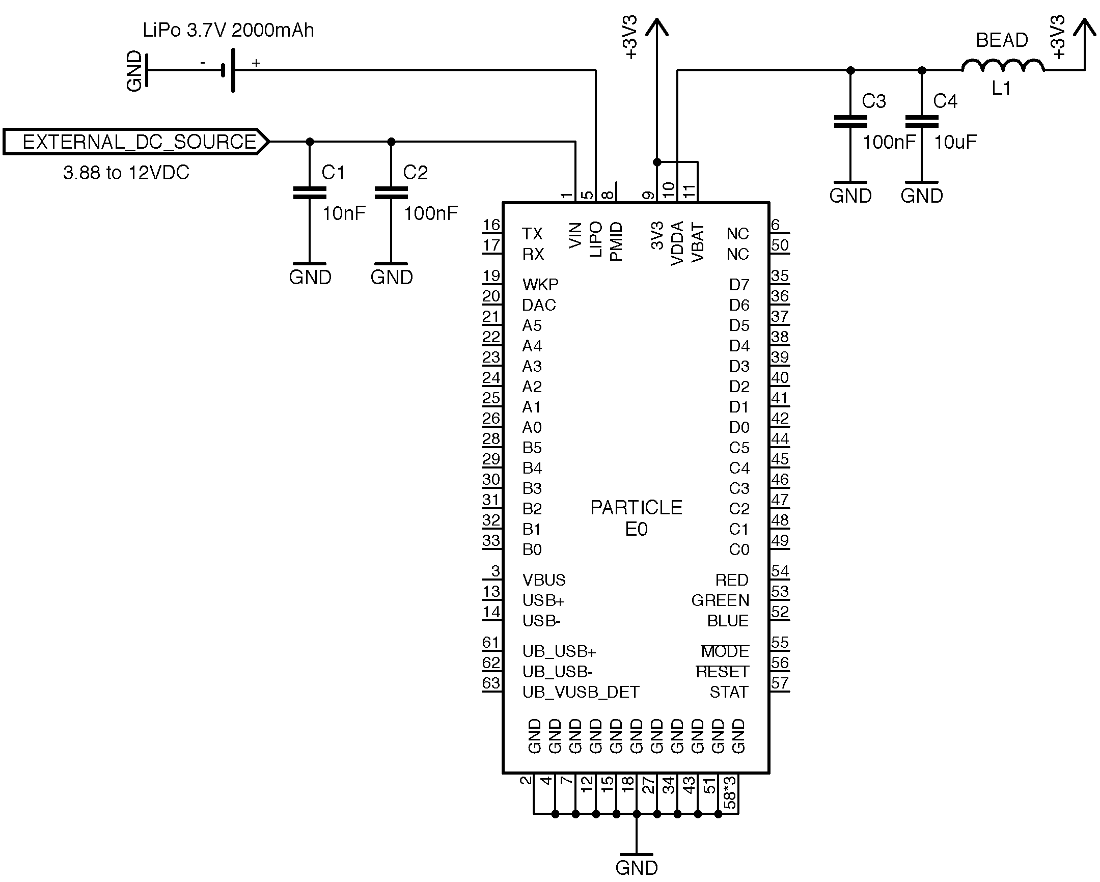
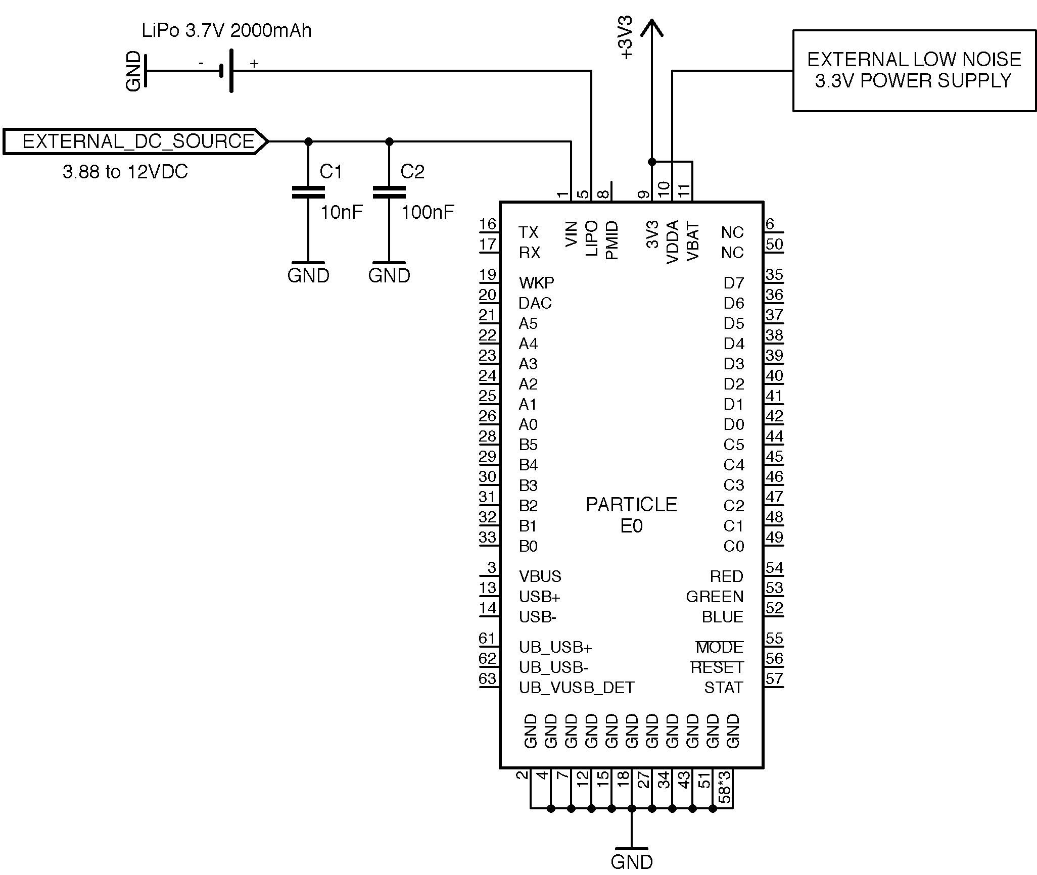
VDDA
This pin powers the analog block of the on board microcontroller. You can connect this directly to the 3V3 pin or power it separately with a low noise power source. In either case, you need to connect it to a source for the module to boot up.
Note: Do not leave this pin unconnected. For the module to boot up, you need to tie this pin to systems 3V3 or other 3.3V supply.
Using an external low-noise power source
VBAT
This is the supply to the internal RTC, backup registers and SRAM. You can connect a backup battery to it (1.65 to 3.6VDC), if you wish to retain RTC/RAM when system supply is removed or simply tie it up to 3V3.
Basic setup
The following is a sample schematic needed to power up and use the E series module. The module is powered over VIN with an external DC power source along with a LiPo battery used as a back up. The RGB LED provides a visual aide to detect the state of the module. Two buttons, RESET and MODE provide the ability to put the module in different modes. LED1 indicates the charging status of the LiPo battery. The main USB port can be used for debugging or to update the firmware on the module.
In addition to these parts, it is also encouraged to add a USB interface for the u-blox module as it provides additional debugging channel and can be used to update the firmware of the modem. The JTAG/SWD interface can be useful to provision the product during manufacturing or when testing/debugging the firmware.
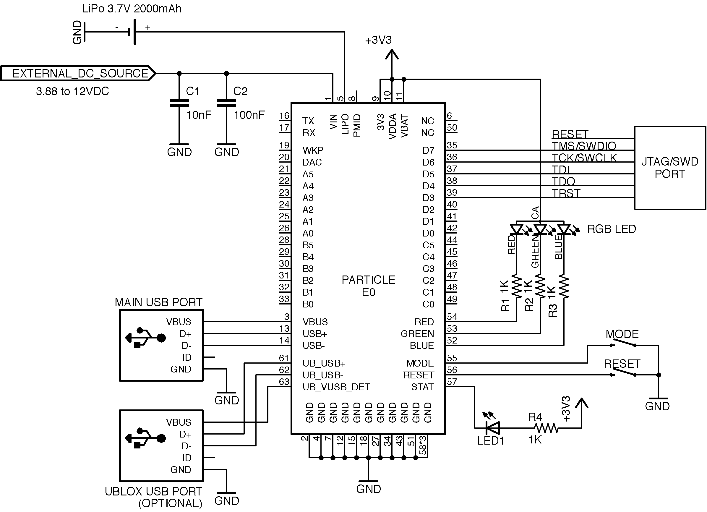
You can also take a look at the schematic and board files of the E series evaluation kit as a reference design available here.
GPIO interface
Electrical parameters
These specifications are based on the STM32F205RGT6 datasheet, with reference to E series pin nomenclature.
| Parameter | Symbol | Conditions | Min | Typ | Max | Unit |
|---|---|---|---|---|---|---|
| Standard I/O input low level voltage | VIL | -0.3 | 0.28*(V3V3-2)+0.8 | V | ||
| I/O FT[1] input low level voltage | VIL | -0.3 | 0.32*(V3V3-2)+0.75 | V | ||
| Standard I/O input high level voltage | VIH | 0.41*(V3V3-2)+1.3 | V3V3+0.3 | V | ||
| I/O FT[1] input high level voltage | VIH | V3V3 > 2V | 0.42*(V3V3-2)+1 | 5.5 | V | |
| VIH | V3V3 ≤ 2V | 0.42*(V3V3-2)+1 | 5.2 | V | ||
| Standard I/O Schmitt trigger voltage hysteresis[2] | Vhys | 200 | mV | |||
| I/O FT Schmitt trigger voltage hysteresis[2] | Vhys | 5% V3V3[3] | mV | |||
| Input leakage current[4] | Ilkg | GND ≤ Vio ≤ V3V3 GPIOs | ±1 | µA | ||
| Input leakage current[4] | Ilkg | RPU | Vio = 5V, I/O FT | 3 | µA | |
| Weak pull-up equivalent resistor[5] | RPU | Vio = GND | 30 | 40 | 50 | k Ω |
| Weak pull-down equivalent resistor[5] | RPD | Vio = V3V3 | 30 | 40 | 50 | k Ω |
| I/O pin capacitance | CIO | 5 | pF | |||
| DAC output voltage (buffers enabled by default) | VDAC | 0.2 | V3V3-0.2 | V | ||
| DAC output resistive load (buffers enabled by default) | RDAC | 5 | k Ω | |||
| DAC output capacitive load (buffers enabled by default) | CDAC | 50 | pF |
Notes:
[1] FT = Five-volt tolerant. In order to sustain a voltage higher than V3V3+0.3 the internal pull-up/pull-down resistors must be disabled.
[2] Hysteresis voltage between Schmitt trigger switching levels. Based on characterization, not tested in production.
[3] With a minimum of 100mV.
[4] Leakage could be higher than max. if negative current is injected on adjacent pins.
[5] Pull-up and pull-down resistors are designed with a true resistance in series with switchable PMOS/NMOS. This PMOS/NMOS contribution to the series resistance is minimum (~10% order).
| Peripheral Type | Qty | Input(I) / Output(O) | FT[1] / 3V3[2] |
|---|---|---|---|
| Digital | 30 | I/O | FT/3V3 |
| Analog (ADC) | 12 | I | 3V3 |
| Analog (DAC) | 2 | O | 3V3 |
| UART | 3 | I/O | 3V3 |
| SPI | 2 | I/O | 3V3 |
| I2S | 1 | I/O | 3V3 |
| I2C | 1 | I/O | FT |
| CAN | 2 | I/O | 3V3[4] |
| USB | 1 | I/O | 3V3 |
| PWM | 133 | O | 3V3 |
Notes: [1] FT = 5.0V tolerant pins. All pins except A3 and DAC are 5V tolerant (when not in analog mode). If used as a 5V input the pull-up/pull-down resistor must be disabled.
[2] 3V3 = 3.3V max pins.
[3] PWM is available on D0, D1, D2, D3, B0, B1, B2, B3, A4, A5, WKP, RX, TX with a caveat: PWM timer peripheral is duplicated on two pins (A5/D2) and (A4/D3) for 11 total independent PWM outputs. For example: PWM may be used on A5 while D2 is used as a GPIO, or D2 as a PWM while A5 is used as an analog input. However A5 and D2 cannot be used as independently controlled PWM outputs at the same time.
[4] Technically these pins are 5.0V tolerant, but since you wouldn't operate them with a 5.0V transceiver it's proper to classify them as 3.3V.
Antenna interface
Antenna interface provided via an IPEX MHF/U.FL receptacle. The interface has LC ESD protection of XXXKV.
Particle recommends the Taoglas PC104 penta-band (850/900/1800/1900/2100 MHz) GSM antenna. The antenna comes with an adhesive backing making it easy to mount. Please refer to its datasheet for further details on power characteristics and optimal placement in a product.
| Antenna Type | Manufacturer | MFG. Part # | Gain |
|---|---|---|---|
| PCB antenna | Taoglas | PC104.07.0165C | 1dBi ~ 2.39dBi |
If you are choosing your own antenna please make sure of the following:
- Optimal support for the operating frequency bands of the module.
- Select an antenna cable with minimum insertion loss.
- Select a connector with 50 ohm impedance.
- Select the antenna with appropriate gain figure that does not exceed the regulatory requirements in the country of operation.
Handling and soldering
ESD precautions
The E series contains highly sensitive electronic circuitry and is an Electrostatic Sensitive Device (ESD). Handling an E series without proper ESD protection may destroy or damage it permanently. Proper ESD handling and packaging procedures must be applied throughout the processing, handling and operation of any application that incorporates the module. ESD precautions should be implemented on the application board where the E series is mounted. Failure to observe these precautions can result in severe damage to the E series!
Packaging
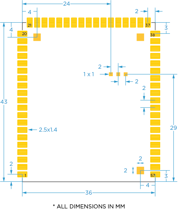
Dimensions and Weight
- Width = 36 mm
- Height = 43 mm
- Thickness = 4.6 mm
- Weight = 8 gms
Pick and place
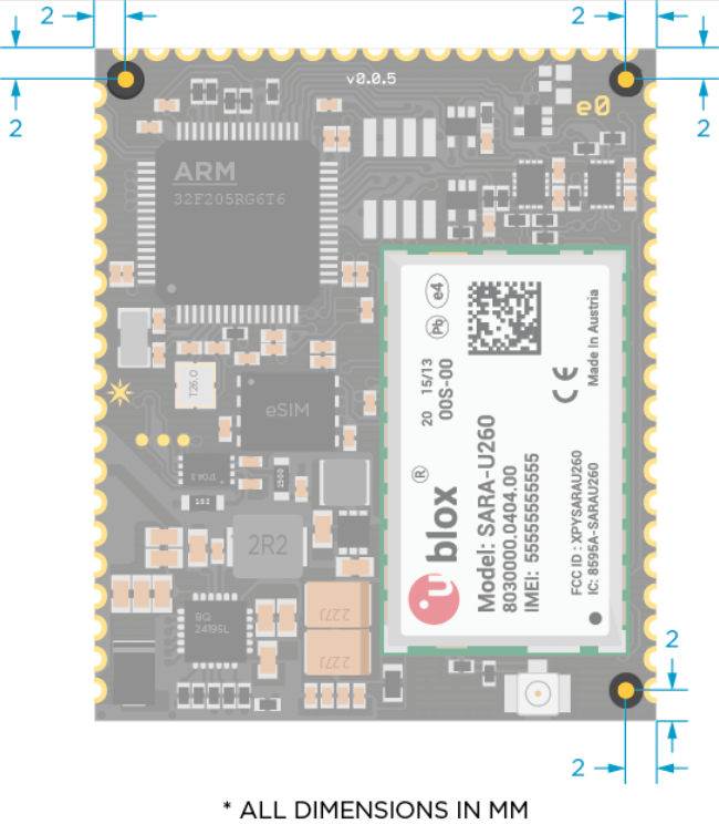
Fiducials
You can use the three fiducials on the top layer for alignment during machine placement of the module.
Soldering
We recommend no clean solder paste over water soluble as it does not require additional cleaning processes.
Alloy specification
- 95.5% Sn / 3.9% Ag / 0.6% Cu (95.5% Tin / 3.9% Silver / 0.6% Copper)
- 95.5% Sn / 4.0% Ag / 0.5% Cu (95.5% Tin / 4.0% Silver / 0.5% Copper)
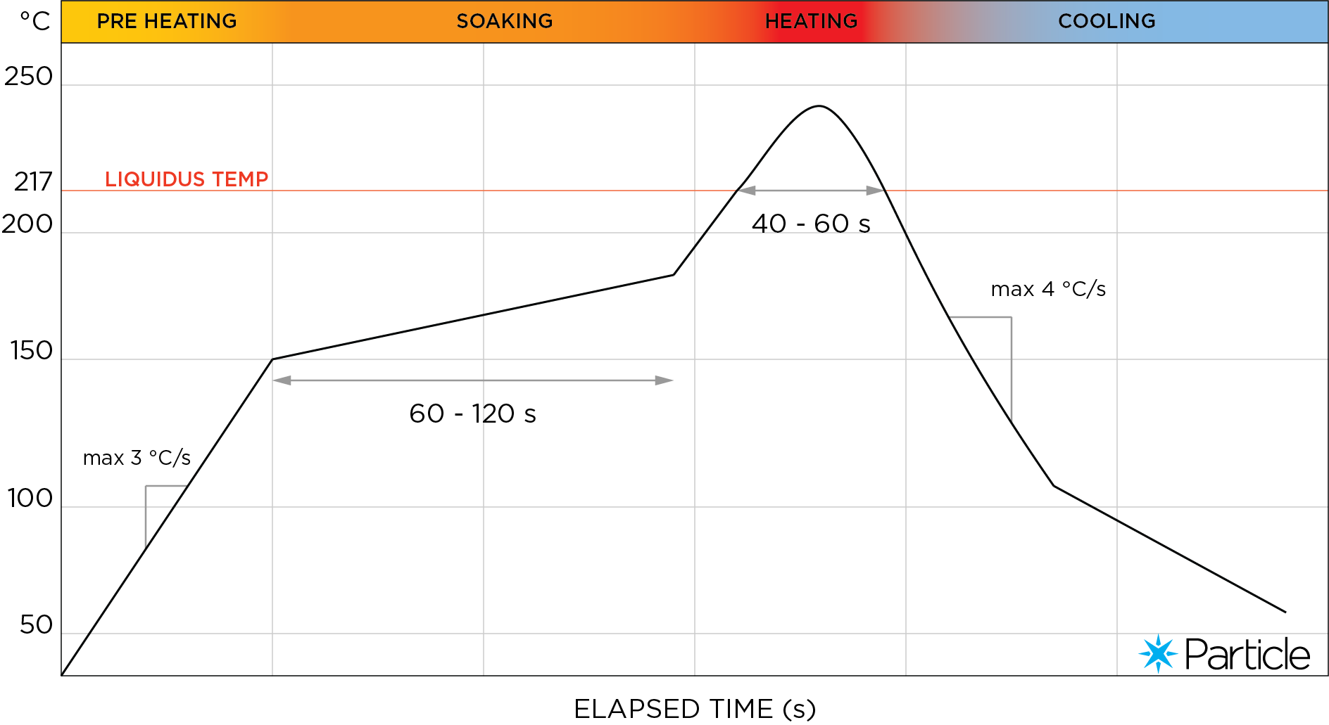
Melting temperature: 217 °C
Stencil thickness: 150 micrometer
Reflow
We recommend a three phase convection reflow oven process. Please refer to IPC-7530 guidelines for in depth details on reflow temperature profiles.
Typical reflow profile for a Pb free solder paste:
Recommended PCB land pattern