
E-Series module datasheet
The E-Series models below have been deprecated. The recommended replacement for the E402/E404 is the E404X.
See the Supply Secure FAQ for more information.
Functional description
Overview
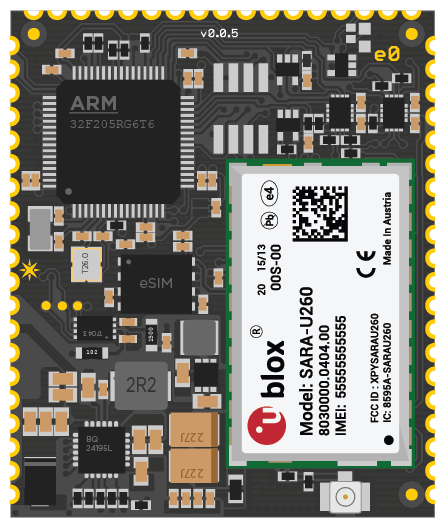
The E-Series module is an IoT platform for creating cellular-connected products. It is an industrial version of Particle's Electron dev kit. It is specifically designed for mass scale manufacturing and integration. It comes with an affordable data plan for low-bandwidth applications. Plus the E-Series is available for more than 100 countries worldwide!
It also comes with Particle's development tools and cloud platform for managing and interacting with your new connected hardware.
Features
- U-blox SARA-U201, SARA-R410M, or SARA-R510S cellular module
- STM32F205RGT6 120MHz ARM Cortex M3 microcontroller
- 1MB flash, 128KB RAM
- BQ24195 power management unit and battery charger
- MAX17043 fuel gauge
- 30 mixed-signal GPIO and advanced peripherals
- Open source software design
- Real-time operation system (RTOS)
- FCC (United States), CE (European Union), and ISED (Canada) certified
- Embedded Particle EtherSIM (E314, E404, E404X)
- Embedded Particle SIM (E310, E402)
Device OS support
It is recommended that you use the latest version in the 2.x LTS release line with the E-Series E310, E313, E314, E402, and E404 (but not the E404X).
While the devices are compatible with older versions of Device OS and 3.x, these versions as past the end-of-support date and are not recommended for use in production. Only 2.x LTS remains in the Extended Support and Maintenance (ESM) window.
For information on upgrading Device OS, see Version information. For the latest version shipped from the factory, see Manufacturing firmware versions page. See also Long Term Support (LTS) releases.
Interfaces
Block diagram
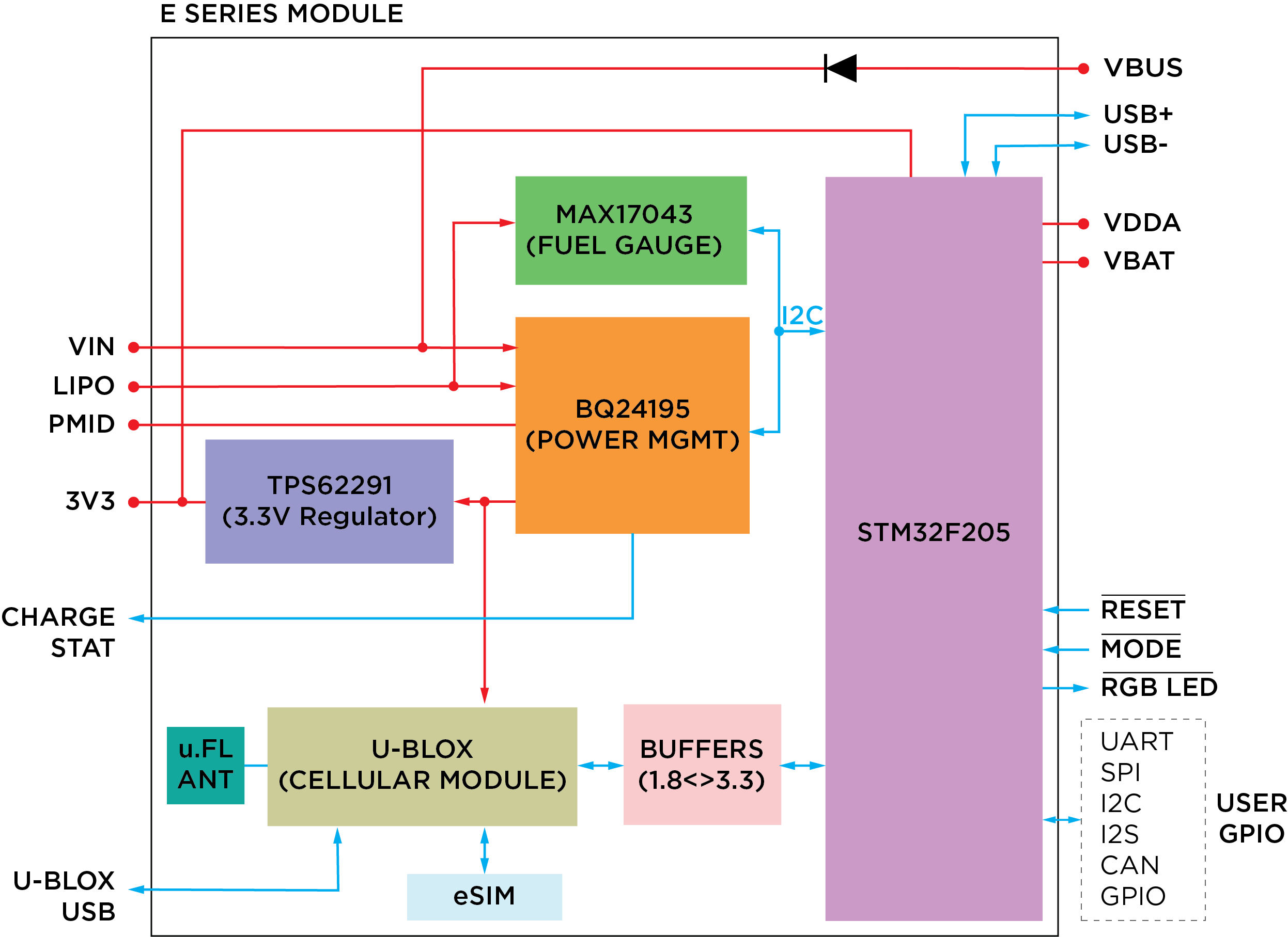
Power
The E series can be powered via the VIN (3.88V-12VDC) pin, over USB, or a LiPo battery.
VIN
The input voltage range on VIN pin is 3.88VDC to 12VDC. When powering from the VIN pin alone, make sure that the power supply is rated at 10W (for example 5 VDC at 2 Amp). If the power source is unable to meet this requirement, you'll need connect the LiPo battery as well. An additional bulk capacitance of 470uF to 1000uF should be added to the VIN input when the LiPo Battery is disconnected. The amount of capacitance required will depend on the ability of the power supply to deliver peak currents to the cellular modem.
The E-Series LTE (E402, LTE Cat M1) can be powered with as little as 550 mA at 5V.
LiPo
This pin serves two purposes. You can use this pin to connect a LiPo battery directly without having to use a JST connector or it can be used to connect an external DC power source (and this is where one needs to take extra precautions). When powering it from an external regulated DC source, the recommended input voltage range on this pin is between 3.6V to 4.4VDC. Make sure that the supply can handle currents of at least 3Amp. This is the most efficient way of powering the E series since the PMIC by-passes the regulator and supplies power to the E series module via an internal FET leading to lower quiescent current.
When powered from a LiPo battery alone, the power management IC switches off the internal regulator and supplies power to the system directly from the battery. This reduces the conduction losses and maximizes battery run time. The battery provided with the E series module is a Lithium-Ion Polymer battery rated at 3.7VDC 1,800mAh. You can substitute this battery with another 3.7V LiPo with higher current rating. Remember to never exceed this voltage rating and always pay attention to the polarity of the connector.
Typical current consumption is around 180mA and up to 1.8A transients at 5VDC. In deep sleep mode, the quiescent current is 130uA (powered from the battery alone).
VBUS
This pin is internally connected to USB supply rail and will output 5V when the E series module is plugged into an USB port. It is intentionally left unpopulated. This pin will NOT output any voltage when the E series module is powered via VIN and/or the LiPo battery.
Most USB ports can supply only a maximum of 500mA, but the u-Blox GSM module on the E series alone can consume a peak of 800mA to 1800mA (2G/3G) or 550 mA (LTE Cat M1) of current during transmission. In order to compensate of this deficit, one must connect the LiPo battery at all times when powering from a traditional USB port for 2G/3G. The E series will intelligently source power from the USB most of the time and keep the battery charged. During peak current requirements, the additional power will be sourced from the battery. This reduces the charge-discharge cycle load on the battery, thus improving its longevity.
3V3 Pin
This pin is the output of the on-board 3.3V switching regulator that powers the microcontroller and the peripherals. This pin can be used as a 3.3V power source with a max load of 800mA. Unlike the Photon or the Core, this pin CANNOT be used as an input to power the E series module.
VDDA
Unlike the Electron, the E series module exposes the VDDA pin of the STM32 microcontroller separately. This pin powers the ADC block of the microcontroller. A maximum difference of 300 mV between VDD (in this case, 3V3) and VDDA can be tolerated during power-up and power-down operation. Under normal operations, connect the VDDA to 3V3 pin of the E0. Be sure to connect VDDA even if you are not using any analog circuitry; the device will fail to boot if not powered.
VBAT
This is the supply to the internal RTC, backup registers and SRAM. You can connect a backup battery to it (1.65 to 3.6VDC), if you wish to retain RTC/RAM when 3V3 is absent or simply tie it up to 3V3.
PMID
This pin is connected to the PMID pin of the bq24195 PMIC. You should leave this pin unconnected.
FCC approved antennas
| Antenna Type | Manufacturer | MFG. Part # | Gain |
|---|---|---|---|
| 2G/3G PCB antenna | Taoglas | PC104.07.0165C | 1dBi ~ 2.39dBi |
| LTE flex antenna | Taoglas | FXUB63.07.0150C | 5.00dBi peak |
Peripherals and GPIO
| Peripheral Type | Qty | Input(I) / Output(O) | FT[1] / 3V3[2] |
|---|---|---|---|
| Digital | 30 | I/O | FT/3V3 |
| Analog (ADC) | 12 | I | 3V3 |
| Analog (DAC) | 2 | O | 3V3 |
| UART | 3 | I/O | 3V3 |
| SPI | 2 | I/O | 3V3 |
| I2S | 1 | I/O | 3V3 |
| I2C | 1 | I/O | FT |
| CAN | 2 | I/O | 3V3[4] |
| USB | 1 | I/O | 3V3 |
| PWM | 133 | O | 3V3 |
Notes: [1] FT = 5.0V tolerant pins. All pins except A3 and DAC are 5V tolerant (when not in analog mode). If used as a 5V input the pull-up/pull-down resistor must be disabled.
[2] 3V3 = 3.3V max pins.
[3] PWM is available on D0, D1, D2, D3, B0, B1, B2, B3, A4, A5, WKP, RX, TX with a caveat: PWM timer peripheral is duplicated on two pins (A5/D2) and (A4/D3) for 11 total independent PWM outputs. For example: PWM may be used on A5 while D2 is used as a GPIO, or D2 as a PWM while A5 is used as an analog input. However A5 and D2 cannot be used as independently controlled PWM outputs at the same time.
[4] Technically these pins are 5.0V tolerant, but since you wouldn't operate them with a 5.0V transceiver it's proper to classify them as 3.3V.
JTAG AND SWD
Pin D3 through D7 are JTAG interface pins. These can be used to reprogram your E series module bootloader or user firmware image with standard JTAG tools such as the ST-Link v2, J-Link, R-Link, OLIMEX ARM-USB-TINI-H, and also the FTDI-based Particle JTAG Programmer. If you are short on available pins, you may also use SWD mode which requires less pins.
| E series module Pin | JTAG | SWD | STM32F205RGT6 Pin | Default Internal[1] |
|---|---|---|---|---|
| D7 | JTAG_TMS | SWD/SWDIO | PA13 | ~40k pull-up |
| D6 | JTAG_TCK | CLK/SWCLK | PA14 | ~40k pull-down |
| D5 | JTAG_TDI | PA15 | ~40k pull-up | |
| D4 | JTAG_TDO | PB3 | Floating | |
| D3 | JTAG_TRST | PB4 | ~40k pull-up | |
| 3V3 | Power | |||
| GND | Ground | |||
| RST | Reset |
Notes:
[1] Default state after reset for a short period of time before these pins are restored to GPIO (if JTAG debugging is not required, i.e. USE_SWD_JTAG=y is not specified on the command line.)
Memory map
STM32F205RGT6 Flash layout overview
- Bootloader (16 KB)
- DCD1 (16 KB), stores keys, mfg info, system flags, etc..
- DCD2 (16 KB), swap area for DCD1
- EEPROM emulation bank 1 (16 KB)
- EEPROM emulation bank 2 (64 KB) [only 16k used]
- Device OS (512 KB) [256 KB comms + 256 KB hal/platform/services]
- Factory backup, OTA backup and user application (384 KB) [3 x 128 KB]
DCD Layout
The DCD area of flash memory has been mapped to a separate DFU media device so that we can incrementally update the application data. This allows one item (say, server public key) to be updated without erasing the other items.
DCD layout as of v0.4.9 found here in firmware
| Region | Offset | Size |
|---|---|---|
| system flags | 0 | 32 |
| version | 32 | 2 |
| device private key | 34 | 1216 |
| device public key | 1250 | 384 |
| ip config | 1634 | 128 |
| claim code | 1762 | 63 |
| claimed | 1825 | 1 |
| device id | 1852 | 6 |
| version string | 1858 | 32 |
| dns resolve | 1890 | 128 |
| reserved1 | 2018 | 64 |
| server public key | 2082 | 768 |
| padding | 2850 | 2 |
| flash modules | 2852 | 100 |
| product store | 2952 | 24 |
| cloud transport | 2977 | 1 |
| alt device public key | 2978 | 128 |
| alt device private key | 3106 | 192 |
| alt server public key | 3298 | 192 |
| alt server address | 3490 | 128 |
| reserved2 | 3618 | 1280 |
Memory map (common)
| Region | Start Address | End Address | Size |
|---|---|---|---|
| Bootloader | 0x8000000 | 0x8004000 | 16 KB |
| DCD1 | 0x8004000 | 0x8008000 | 16 KB |
| DCD2 | 0x8008000 | 0x800C000 | 16 KB |
| EEPROM1 | 0x800C000 | 0x8010000 | 16 KB |
| EEPROM2 | 0x8010000 | 0x8020000 | 64 KB |
Memory map (modular firmware - default)
Before 0.6.0 firmware
| Region | Start Address | End Address | Size |
|---|---|---|---|
| System Part 1 | 0x8020000 | 0x8040000 | 128 KB |
| System Part 2 | 0x8040000 | 0x8060000 | 128 KB |
| Application | 0x8080000 | 0x80A0000 | 128 KB |
| Factory Reset/Extended Application | 0x80A0000 | 0x80C0000 | 128 KB |
| OTA Backup | 0x80C0000 | 0x80E0000 | 128 KB |
| Decompress region | 0x80E0000 | 0x8100000 | 128 KB |
Since 0.6.0 firmware
| Region | Start Address | End Address | Size |
|---|---|---|---|
| System Part 2 | 0x8020000 | 0x8040000 | 128 KB |
| System Part 3 | 0x8040000 | 0x8060000 | 128 KB |
| System Part 1 | 0x8060000 | 0x8080000 | 128 KB |
| Application | 0x8080000 | 0x80A0000 | 128 KB |
| Factory Reset/Extended Application | 0x80A0000 | 0x80C0000 | 128 KB |
| OTA Backup | 0x80C0000 | 0x80E0000 | 128 KB |
| Decompress region | 0x80E0000 | 0x8100000 | 128 KB |
Memory map (monolithic firmware - optional)
| Region | Start Address | End Address | Size |
|---|---|---|---|
| Firmware | 0x8020000 | 0x8080000 | 384 KB |
| Factory Reset | 0x8080000 | 0x80E0000 | 384 KB |
| Unused (factory reset modular) | 0x80E0000 | 0x8100000 | 128 KB |
Pin and button definition
Pin markings:
LED Status
Charge status LED
| State | Description |
|---|---|
| ON | Charging in progress |
| OFF | Charging complete |
| Blink at 1Hz | Fault condition[1] |
| Rapid blinking | Battery disconnected[2] |
Notes:
[1] A fault condition can occur due to several reasons, for example, battery over/under voltage, temperature fault or safety timer fault. You can find the root cause by reading the fault register of the power management IC in firmware.
[2] You can stop this behavior by either plugging in the LiPo battery or by disabling the charging using the appropriate firmware command.
System RGB LED
Unlike the Electron, the E series module does not have an on-board RGB status LED. We have provided its individual control pins for you to connect an LED of your liking. This will allow greater flexibility in the end design of your products.
For a detailed explanation of different color codes of the RGB system LED, please take a look here.
Pinout diagram

You can download a high resolution pinout diagram in a PDF version here.
Pin description
| # | PIN | FUNCTION | DESCRIPTION |
|---|---|---|---|
| 1 | VIN | POWER | This pin can be used as an input or output. As an input, supply 5VDC to 12VDC to power the Electron. When the Electron is powered via the USB port, this pin will output a voltage of approximately 4.8VDC due to a reverse polarity protection series Schottky diode between VBUS and VIN. When used as an output, the max load on VIN is 1Amp. |
| 2 | GND | POWER | System ground. |
| 3 | VBUS | POWER | This is connected to the VBUS power pin of the USB port. |
| 4 | GND | POWER | System ground. |
| 5 | LIPO | POWER | This is connected to the +LiPo connector. |
| 6 | NC | TBD | Do not connect. |
| 7 | GND | POWER | System ground. |
| 8 | PMID | POWER | This is connected to the PMID pin of the PMIC. |
| 9 | 3V3 | POWER | This is the output of the 3V3 regulator on the E0. |
| 10 | VDDA | POWER | This is the input to the analog block of the STM32. |
| 11 | VBAT | POWER | Supply to the internal RTC, backup registers and SRAM when 3V3 is not present (1.65 to 3.6VDC). |
| 12 | GND | POWER | System ground. |
| 13 | USB+ | IO | Data+ pin of the USB port. |
| 14 | USB- | IO | Data- pin of the USB port. |
| 15 | GND | POWER | System ground. |
| 16 | TX | IO | Primarily used as UART TX, but can also be used as a digital GPIO or PWM. |
| 17 | RX | IO | Primarily used as UART RX, but can also be used as a digital GPIO or PWM. |
| 18 | GND | POWER | System ground. |
| 19 | WKP | IO | Active-high wakeup pin, wakes the module from sleep/standby modes. When not used as a WAKEUP, this pin can also be used as a digital GPIO, ADC input or PWM. Can be referred to as A7 when used as an ADC. |
| 20 | DAC | IO | 12-bit Digital-to-Analog (D/A) output (0-4095), referred to as DAC or DAC1 in software. Can also be used as a digital GPIO or ADC. Can be referred to as A6 when used as an ADC. |
| 21 | A5 | IO | 12-bit Analog-to-Digital (A/D) inputs (0-4095), and also digital GPIOs. |
| 22 | A4 | IO | 12-bit Analog-to-Digital (A/D) inputs (0-4095), and also digital GPIOs. |
| 23 | A3 | IO | 12-bit Analog-to-Digital (A/D) inputs (0-4095), and also digital GPIOs. |
| 24 | A2 | IO | 12-bit Analog-to-Digital (A/D) inputs (0-4095), and also digital GPIOs. |
| 25 | A1 | IO | 12-bit Analog-to-Digital (A/D) inputs (0-4095), and also digital GPIOs. |
| 26 | A0 | IO | 12-bit Analog-to-Digital (A/D) inputs (0-4095), and also digital GPIOs. |
| 27 | GND | POWER | System ground. |
| 28 | B5 | IO | 12-bit Analog-to-Digital (A/D) inputs (0-4095), and also digital GPIOs. |
| 29 | B4 | IO | 12-bit Analog-to-Digital (A/D) inputs (0-4095), and also digital GPIOs. |
| 30 | B3 | IO | 12-bit Analog-to-Digital (A/D) inputs (0-4095), PWM and also digital GPIOs. |
| 31 | B2 | IO | 12-bit Analog-to-Digital (A/D) inputs (0-4095), PWM and also digital GPIOs. |
| 32 | B1 | IO | Digital only GPIO, and PWM. |
| 33 | B0 | IO | Digital only GPIO, and PWM. |
| 34 | GND | POWER | System ground. |
| 35 | D7 | IO | Digital only GPIO. |
| 36 | D6 | IO | Digital only GPIO. |
| 37 | D5 | IO | Digital only GPIO. |
| 38 | D4 | IO | Digital only GPIO. |
| 39 | D3 | IO | Digital only GPIO, and PWM. |
| 40 | D2 | IO | Digital only GPIO, and PWM. |
| 41 | D1 | IO | Digital only GPIO, and PWM. |
| 42 | D0 | IO | Digital only GPIO, and PWM. |
| 43 | GND | POWER | System ground. |
| 44 | C5 | IO | Digital only GPIO, and PWM. |
| 45 | C4 | IO | Digital only GPIO, and PWM. |
| 46 | C3 | IO | Digital only GPIO. |
| 47 | C2 | IO | Digital only GPIO. |
| 48 | C1 | IO | Digital only GPIO. |
| 49 | C0 | IO | Digital only GPIO. |
| 50 | NC | TBD | Do not connect. |
| 51 | GND | POWER | System ground. |
| 52 | BLU | IO | Blue pin of the RGB LED. |
| 53 | GRN | IO | Green pin of the RGB LED. |
| 54 | RED | IO | Red pin of the RGB LED. |
| 55 | MODE | IO | Connected to the MODE button input. |
| 56 | RST | I | Active-low reset input. |
| 57 | STAT | O | Connected to the charge status pin of the PMIC. |
| 58 | GND | POWER | System ground. |
| 59 | GND | POWER | System ground. |
| 60 | GND | POWER | System ground. |
| 61 | UB_USB+ | IO | Data+ pin of the u-blox USB port. |
| 62 | UB_USB- | IO | Data- pin of the u-blox USB port. |
| 63 | UB_VUSB_DET | IO | USB detect pin of the u-blox USB port. 5V on this pin enables the u-blox's USB interface. |
[1] PWM is available on D0, D1, D2, D3, B0, B1, B2, B3, A4, A5, WKP, RX, TX with a caveat: PWM timer peripheral is duplicated on two pins (A5/D2) and (A4/D3) for 11 total independent PWM outputs. For example: PWM may be used on A5 while D2 is used as a GPIO, or D2 as a PWM while A5 is used as an analog input. However A5 and D2 cannot be used as independently controlled PWM outputs at the same time.
Technical specifications
Absolute maximum ratings [1]
| Parameter | Symbol | Min | Typ | Max | Unit |
|---|---|---|---|---|---|
| Supply Input Voltage | VIN-MAX | +17 | V | ||
| Supply Output Current | IIN-MAX-L | 1 | A | ||
| Battery Input Voltage | VLiPo | +6 | V | ||
| Supply Output Current | I3V3-MAX-L | 800 | mA | ||
| Storage Temperature | Tstg | -30 | +75 | °C | |
| ESD Susceptibility HBM (Human Body Mode) | VESD | 2 | kV |
[1] Stresses beyond those listed under absolute maximum ratings may cause permanent damage to the device. These are stress ratings only, and functional operation of the device at these or any other conditions beyond those indicated under recommended operating conditions is not implied. Exposure to absolute-maximum-rated conditions for extended periods may affect device reliability.
Recommended operating conditions
| Parameter | Symbol | Min | Typ | Max | Unit |
|---|---|---|---|---|---|
| Supply Input Voltage | VIN | +3.88[1] | +12 | V | |
| Supply Output Voltage | VIN | +4.8 | V | ||
| Supply Output Voltage | V3V3 | +3.3 | V | ||
| LiPo Battery Voltage | VLiPo | +3.6 | +4.4 | V | |
| Supply Input Voltage | VVBAT | +1.65 | +3.6 | V | |
| Supply Input Current (VBAT) | IVBAT | 19 | uA | ||
| Operating Current (uC on, Cellular ON) | IIN avg | 180 | 250 | mA | |
| 2G/3G Peak Current (uC on, Cellular ON) | IIN pk | 800[2] | 1800[3] | mA | |
| LTE Peak Current (uC on, Cellular ON) | IIN pk | 550 | mA | ||
| Operating Current (uC on, Cellular OFF) | IIN avg | 47 | 50 | mA | |
| Sleep Current (4.2V LiPo, Cellular OFF) | IQs | 0.8 | 2 | mA | |
| Deep Sleep Current (4.2V LiPo, Cellular OFF) | IQds | 110 | 130 | uA | |
| Operating Temperature | Top | -40[4] | +85[4] | °C | |
| Humidity Range Non condensing, relative humidity | 95 | % |
Notes:
[1] The minimum input voltage is software defined with a user selectable range of 3.88V to 5.08V in 80mV increments. Out of the box, the minimum input voltage is set to 4.36V in order for the LiPo battery to be able to properly charge.
[2] 3G operation
[3] 2G operation
[4] When powering the E series module with a LiPo battery (or other battery chemistries), please note that the operating temperatures will be affected accordingly.
Radio specifications
The E series is available in two different versions: A 2G/3G global model (SARA-U201) and a LTE Cat M1 model (SARA-R410M-02B).
Note that LTE is LTE Cat M1, not the standard LTE (LTE Cat 1) used by your mobile phone. It is a low-power and low-data-rate variation of LTE for use with IoT devices. It can only be used in the United States, Canada. and Mexico at this time.
For a complete list of carriers and supported countries, see the carrier guide.
2G cellular characteristics E314 & E310:
| Parameter | SARA-U201 |
|---|---|
| Protocol stack | 3GPP Release 7 |
| MS Class | Class B |
| Bands | GSM 850 MHz |
| E-GSM 900 MHz | |
| DCS 1800 MHz | |
| PCS 1900 MHz | |
| Power Class | Class 4 (33 dBm) for 850/900 bands |
| Class 1 (30 dBm) for 1800/1900 bands |
3G cellular characteristics E314 & E310:
| Parameter | SARA-U201 |
|---|---|
| Protocol stack | 3GPP Release 7 |
| UE Class | Class A |
| Bands | Band 5 (850 MHz) |
| Band 8 (900 MHz) | |
| Band 2 (1900 MHz) | |
| Band 1 (2100 MHz) | |
| Power Class | Class 3 (24 dBm) for all bands |
u-blox SARA-R410M-02B-00 or R410M-02B-03
| Parameter | Value |
|---|---|
| Protocol stack | 3GPP Release 13 |
| RAT | LTE Cat M1 Half-Duplex |
| LTE FDD Bands | Band 12 (700 MHz) |
| Band 28 (700 MHz) | |
| Band 13 (750 MHz) | |
| Band 20 (800 MHz) | |
| Band 5 (850 MHz) | |
| Band 8 (900 MHz) | |
| Band 4 (1700 MHz) | |
| Band 3 (1800 MHz) | |
| Band 2 (1900 MHz) | |
| Power class | Class 3 (23 dBm) |
u-blox SARA-R510S-01B
| Parameter | Value |
|---|---|
| Protocol stack | 3GPP Release 13 |
| RAT | LTE Cat M1 Half-Duplex |
| LTE FDD Bands | Band 12 (700 MHz) |
| Band 13 (750 MHz) | |
| Band 26 (850 MHz) | |
| Band 5 (850 MHz) | |
| Band 4 (1700 MHz) | |
| Band 2 (1900 MHz) | |
| Band 25 (1900 MHz) | |
| Power class | Class 3 (23 dBm) |
I/O characteristics
These specifications are based on the STM32F205RGT6 datasheet, with reference to E series pin nomenclature.
| Parameter | Symbol | Conditions | Min | Typ | Max | Unit |
|---|---|---|---|---|---|---|
| Standard I/O input low level voltage | VIL | -0.3 | 0.28*(V3V3-2)+0.8 | V | ||
| I/O FT[1] input low level voltage | VIL | -0.3 | 0.32*(V3V3-2)+0.75 | V | ||
| Standard I/O input high level voltage | VIH | 0.41*(V3V3-2)+1.3 | V3V3+0.3 | V | ||
| I/O FT[1] input high level voltage | VIH | V3V3 > 2V | 0.42*(V3V3-2)+1 | 5.5 | V | |
| VIH | V3V3 ≤ 2V | 0.42*(V3V3-2)+1 | 5.2 | V | ||
| Standard I/O Schmitt trigger voltage hysteresis[2] | Vhys | 200 | mV | |||
| I/O FT Schmitt trigger voltage hysteresis[2] | Vhys | 5% V3V3[3] | mV | |||
| Input leakage current[4] | Ilkg | GND ≤ Vio ≤ V3V3 GPIOs | ±1 | µA | ||
| Input leakage current[4] | Ilkg | RPU | Vio = 5V, I/O FT | 3 | µA | |
| Weak pull-up equivalent resistor[5] | RPU | Vio = GND | 30 | 40 | 50 | k Ω |
| Weak pull-down equivalent resistor[5] | RPD | Vio = V3V3 | 30 | 40 | 50 | k Ω |
| I/O pin capacitance | CIO | 5 | pF | |||
| DAC output voltage (buffers enabled by default) | VDAC | 0.2 | V3V3-0.2 | V | ||
| DAC output resistive load (buffers enabled by default) | RDAC | 5 | k Ω | |||
| DAC output capacitive load (buffers enabled by default) | CDAC | 50 | pF |
Notes:
[1] FT = Five-volt tolerant. In order to sustain a voltage higher than V3V3+0.3 the internal pull-up/pull-down resistors must be disabled.
[2] Hysteresis voltage between Schmitt trigger switching levels. Based on characterization, not tested in production.
[3] With a minimum of 100mV.
[4] Leakage could be higher than max. if negative current is injected on adjacent pins.
[5] Pull-up and pull-down resistors are designed with a true resistance in series with switchable PMOS/NMOS. This PMOS/NMOS contribution to the series resistance is minimum (~10% order).
Mechanical specifications
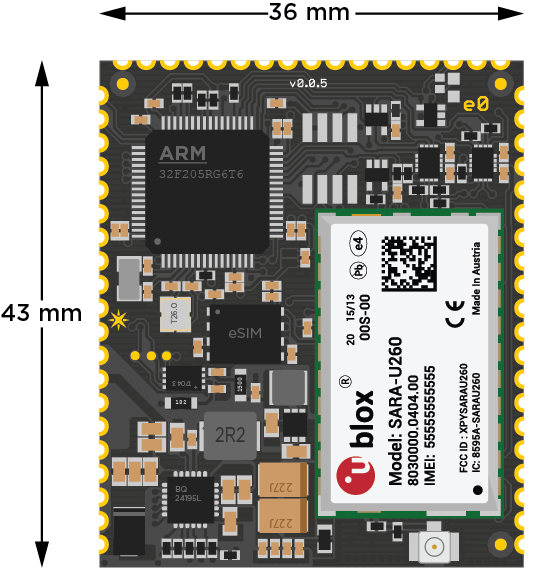
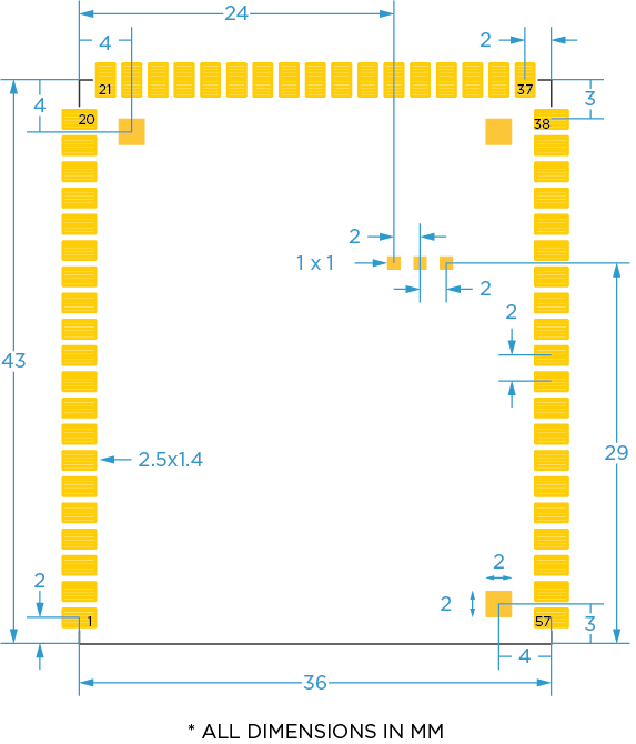
Dimensions and weight
- Width = 36 mm
- Height = 43 mm
- Thickness = 4.6 mm
- Weight = 8 gms
Recommended PCB land pattern
An E series part for EAGLE can be found in the Particle EAGLE library
Schematics
USB
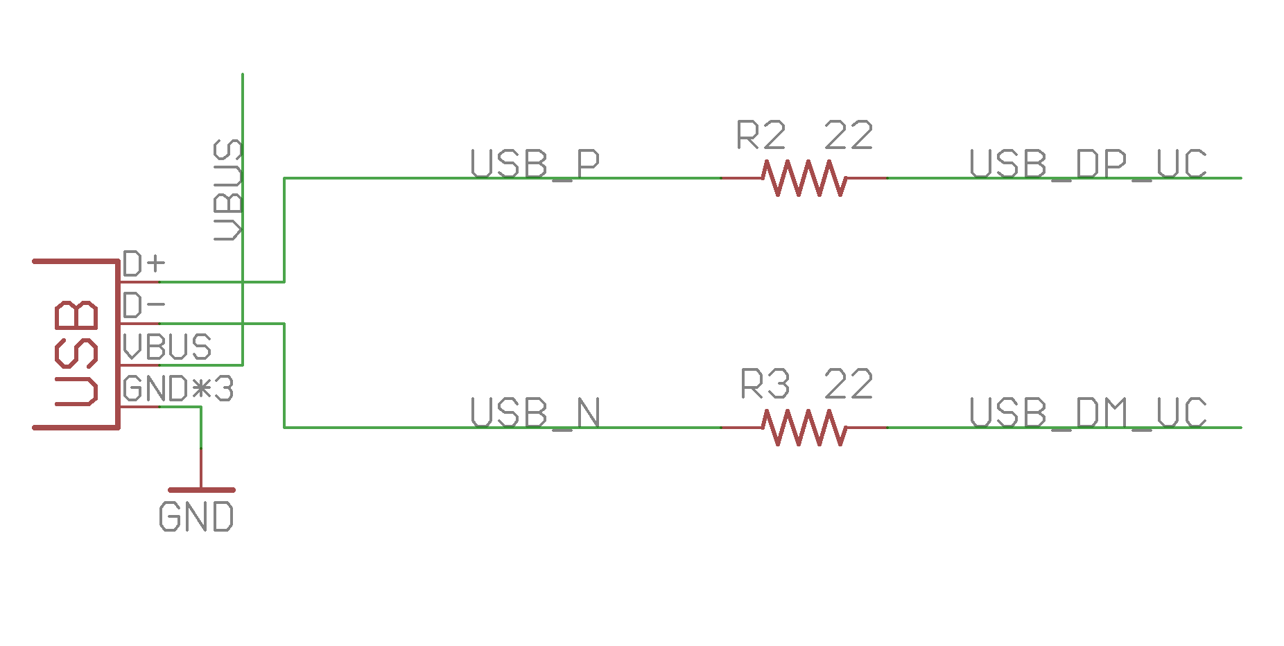
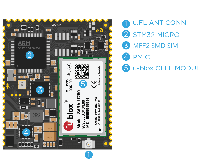
The USB data lines are terminated with 22 Ohm resistors. These data pins are also exposed via small through holes next to the USB connector and are labeled D+ and D-. The VBUS (+5VDC VCC of the USB port) is fed to the PMIC via a 3Amp Schottky diode (SS3P3). The VBUS pin is also available via the unpopulated header hole on the top-right side of the E series.
PMIC (Power management integrated circuit)
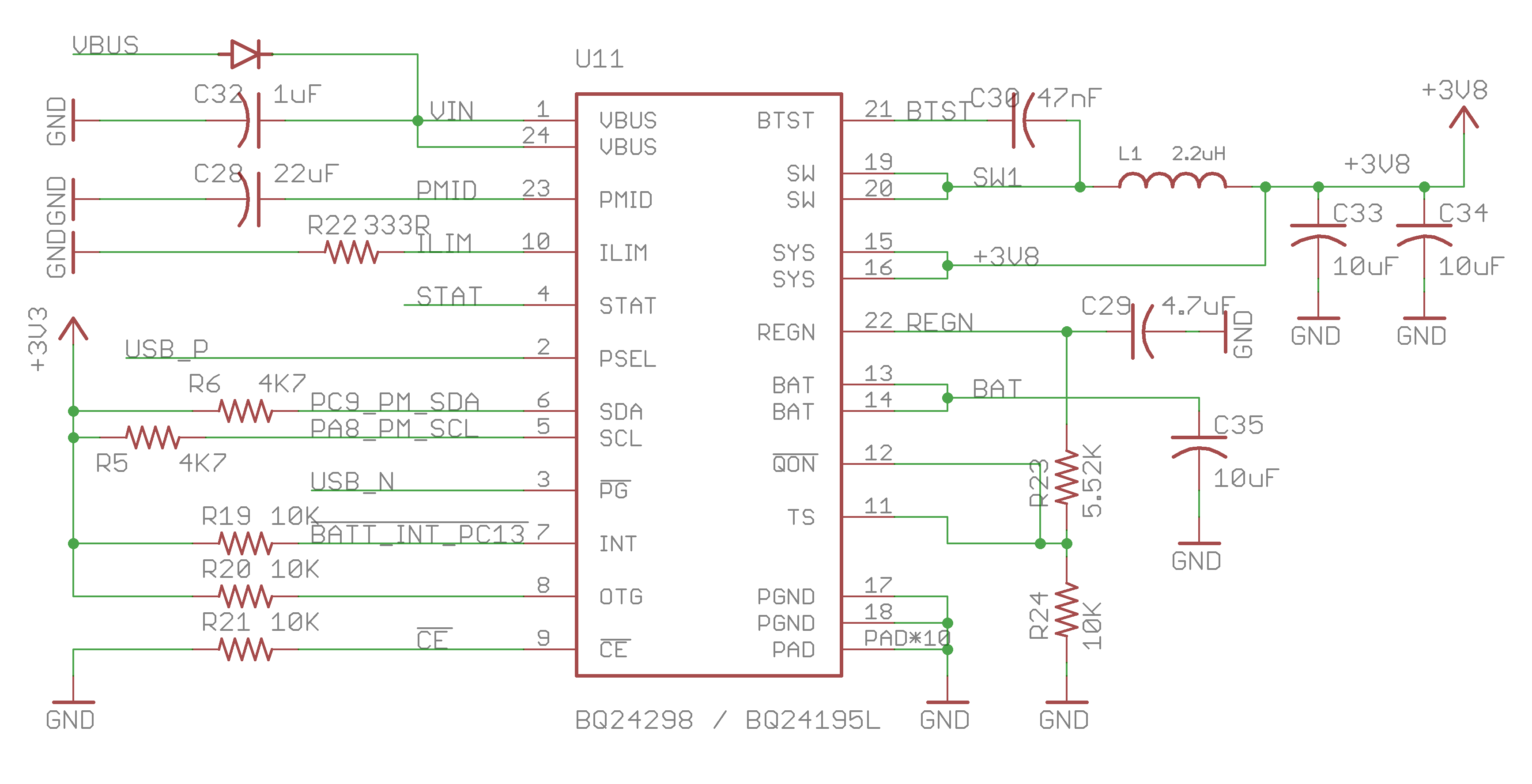
The E series uses TI's BQ24195 as the power management and charging unit. This PMIC intelligently sources power from either the VIN pin, the USB port and/or the LiPo battery. When all the power sources as connected, the unit tries to source power from the USB or VIN as default and continues to charge the LiPo battery. When the battery is completely charged, the power is then sourced from USB/VIN alone. If there is a power deficit (which generally occurs during cellular radio transmission), the additional power is then sourced from the battery as required. The unit can also seamlessly switch back to the battery when other sources of power are suddenly removed.
The DP data pin of the USB is used by the PMIC to detect the presence of a USB power source. It then adjusts the charge current and the limit based on the type of USB power source it detects. This does not always happen successfully since there are a lot of USB hubs and chargers out there that do not meet the USB design guidelines. If the detection is unsuccessful, the PMIC defaults to a 500mA current limit. A user can always adjust these parameters via software.
The microcontroller communicates with the PMIC via an I2C interface (pins PC9 and PA8). This interface allows the microcontroller to read the status of the PMIC and set its various parameters.
Microcontroller
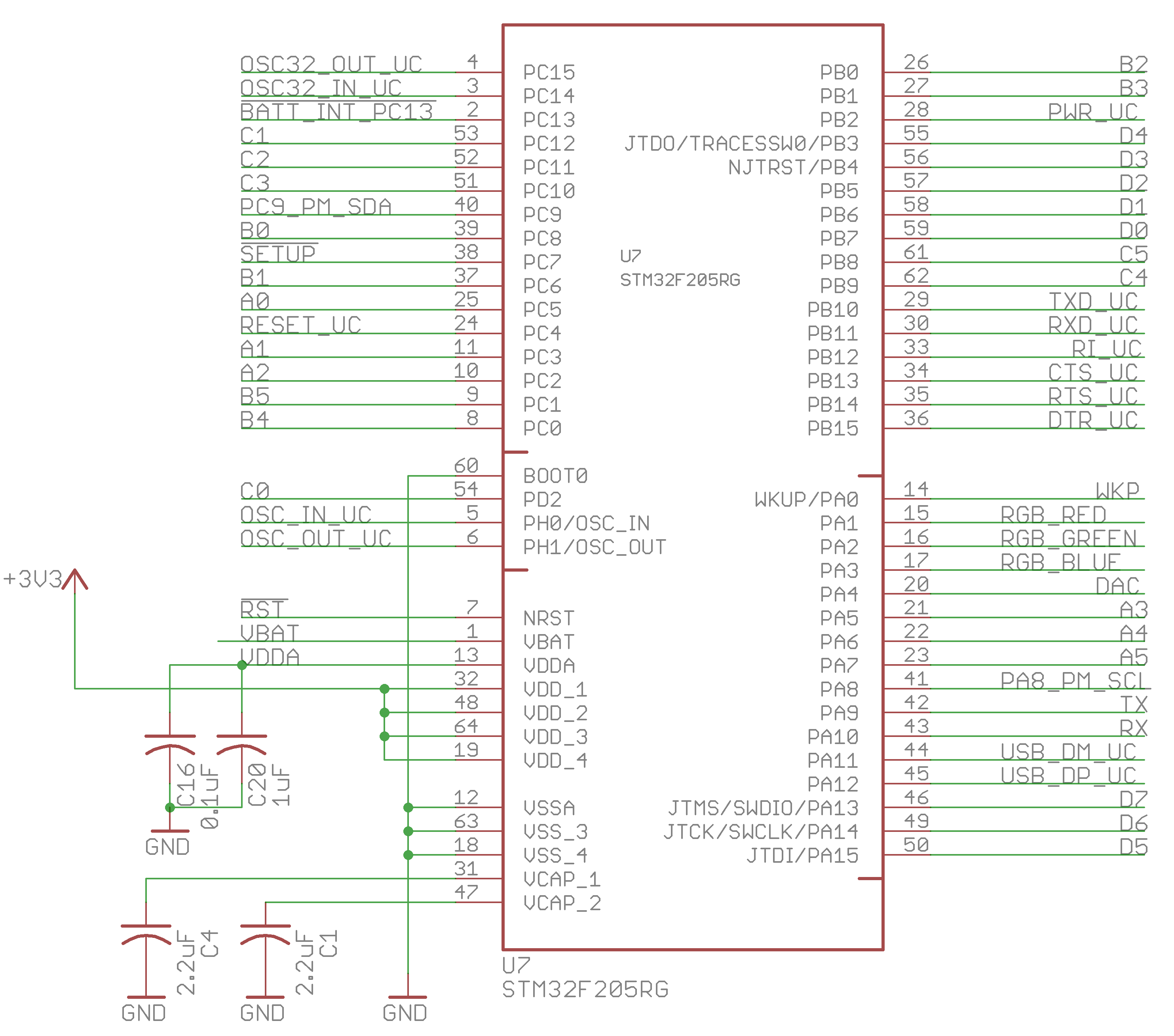
The E series uses ST Microelectronics's STM32F205RGT6 ARM Cortex M3 microcontroller running at 120MHz.
U-blox cellular module
The u-blox cellular module talks to the microcontroller over a full-duplex USART interface using a standard set of AT commands. The MFF2 embedded SIM chip is directly connected to the u-blox module.
The MFF2 SMD SIM is not an e-sim and is not reprogrammable to other carriers. It's set to the Particle MVNO and cannot be changed.
Buffers
Since u-blox module's communication interface operates at 1.8VDC, while the STM32F205RGT6 microcontroller operates at 3.3VDC, we need voltage translators in-between them. This is achieved with two SN74AVC4T245 non-inverting buffers. The default state of the USART pins is set with the help of pull-up and pull-down resistors, and the unused input pins are tied to GND.
3.3V regulator and fuel gauge
The output (3.8V net) of the PMIC is fed directly to the u-blox cellular module and a 3.3VDC high efficiency switching regulator (TPS62290). This 3.3VDC regulator helps power the microcontroller, fuel gauge and the buffers.
The E series employs a MAX17043 fuel gauge to monitor the LiPo battery voltage and it's state of charge. The microcontroller communicates with it over an I2C interface (same channel as the PMIC).
Product variants
| Name | Connectivity | Geography | u-blox variant | Band Support |
|---|---|---|---|---|
| E314 | 3G with 2G fallback (EtherSIM) | Global | SARA-U201 | 850/900/1800/1900/2100 MHz |
| E310 | 3G with 2G fallback (pre-2021) | Global | SARA-U201 | 850/900/1800/1900/2100 MHz |
| E404X | LTE M1 only (EtherSIM) | US, Canada, Mexico | R510S-01B | LTE M1: 1, 2, 3, 4, 5, 8, 12, 13, 18, 19, 20, 25, 26, 28 |
| E404 | LTE M1 only (EtherSIM) | US, Canada, Mexico | R410M-02B or -03 | LTE M1: 1, 2, 3, 4, 5, 8, 12, 13, 20, 25, 26, 28, 39 |
| E402 | LTE M1 only (pre-2021) | US, Canada, Mexico | R410M-02B | LTE M1: 1, 2, 3, 4, 5, 8, 12, 13, 20, 25, 26, 28, 39 |
Country compatibility
| Country | Model | Technologies | Carriers |
|---|---|---|---|
| Afghanistan | E314 | 2G, 3G | MTN |
| Albania | E314 | 2G, 3G | Eagle, Telekom, Vodafone |
| Algeria | E314 | 2G, 3G | Mobilis, Ooredoo |
| Anguilla | E314 | 2G, 3G | Flow |
| Antigua and Barbuda | E314 | 2G, 3G | Flow |
| Argentina | E314 | 2G, 3G | Claro, Movistar, Personal |
| Armenia | E314 | 2G, 3G | Beeline, Ucom |
| Aruba | E314 | 2G, 3G | Setar |
| Austria | E314 | 2G | 3 (Drei), A1, T-Mobile |
| Azerbaijan | E314 | 2G, 3G | Azercell, Bakcell, NAR Mobile |
| Bahamas | E314 | 2G, 3G | Aliv, BTC Bahamas |
| Bahrain | E314 | 2G | Zain |
| Bangladesh | E314 | 2G, 3G | Bangalink, GrameenPhone |
| Barbados | E314 | 2G, 3G | Flow |
| Belarus | E314 | 2G, 3G | A1 |
| Belgium | E314 | 2G | Base, Orange, Proximus |
| Belize | E314 | 3G | Smart |
| Bolivia | E314 | 2G, 3G | Viva |
| Bosnia and Herzegovina | E314 | 2G, 3G | HT Eronet |
| Brunei | E314 | 3G | DST |
| Bulgaria | E314 | 2G, 3G | A1, Telenor, Vivacom |
| Burkina Faso | E314 | 2G, 3G | Orange |
| Cambodia | E314 | 2G, 3G | Metfone |
| Canada | E404 | M1 | Bell Mobility, Rogers Wireless, Telus |
| Cayman Islands | E314 | 2G, 3G | Flow |
| Chad | E314 | 2G, 3G | Airtel |
| Chile | E314 | 3G | Entel, Movistar |
| Colombia | E314 | 2G, 3G | Movistar, Tigo |
| Congo (Brazzaville) | E314 | 2G, 3G | Airtel |
| Congo (Kinshasa) | E314 | 2G, 3G | Airtel |
| Costa Rica | E314 | 3G | Movistar |
| Côte d'Ivoire | E314 | 2G, 3G | MTN |
| Croatia | E314 | 2G, 3G | Hrvatski Telekom, Tele2 |
| Cyprus | E314 | 2G, 3G | MTN |
| Czechia | E314 | 2G | T-Mobile, Vodafone |
| Denmark | E314 | 2G | TDC, Telenor, Telia |
| Dominica | E314 | 2G, 3G | Flow |
| Dominican Republic | E314 | 2G, 3G | Altice Dominicana, Viva |
| Ecuador | E314 | 2G, 3G | Claro, Movistar |
| Egypt | E314 | 2G, 3G | Etisalat, Orange |
| El Salvador | E314 | 2G, 3G | Claro, Telefonica |
| Estonia | E314 | 2G, 3G | Elisa, Tele2, Telia |
| eSwatini | E314 | 2G, 3G | MTN |
| Ethiopia | E314 | 2G, 3G | Ethio Telecom |
| Faroe Islands | E314 | 2G, 3G | Faroese Telecom, Vodafone |
| Finland | E314 | 2G | Elisa |
| France | E314 | 2G, 3G | Bouygues, Free Mobile, Orange, SFR |
| French Guiana | E314 | 2G, 3G | Digicel |
| Gabon | E314 | 2G, 3G | Airtel |
| Georgia | E314 | 2G, 3G | Beeline, Geocell |
| Germany | E314 | 2G | O2, Telekom |
| Ghana | E314 | 2G, 3G | AirtelTigo, MTN |
| Gibraltar | E314 | 2G, 3G | Gibtel |
| Greece | E314 | 2G | Cosmote, Wind |
| Grenada | E314 | 2G | Flow |
| Guadeloupe | E314 | 2G, 3G | Orange |
| Guatemala | E314 | 2G, 3G | Claro, Movistar |
| Guinea | E314 | 2G, 3G | MTN |
| Guinea-Bissau | E314 | 2G, 3G | MTN |
| Guyana | E314 | 2G | Digicel |
| Haiti | E314 | 2G, 3G | Digicel |
| Honduras | E314 | 2G, 3G | Claro, Tigo |
| Hong Kong | E314 | 3G | CSL, SmarTone |
| Hungary | E314 | 2G, 3G | Telenor |
| Indonesia | E314 | 2G | Indosat, Telkomsel, XL Axiata |
| Ireland | E314 | 2G, 3G | Meteor, O2, Vodafone |
| Italy | E314 | 2G | TIM, Vodafone, Wind |
| Jordan | E314 | 2G, 3G | Zain |
| Kazakhstan | E314 | 2G, 3G | Beeline, K-Cell |
| Kenya | E314 | 2G, 3G | Airtel |
| Kuwait | E314 | 2G, 3G | Viva, Zain |
| Kyrgyzstan | E314 | 2G | Beeline |
| Latvia | E314 | 2G | Bite, LMT, Tele2 |
| Liechtenstein | E314 | 2G, 3G | Mobilkom, Orange |
| Lithuania | E314 | 2G | Bite, Omnitel, Tele2 |
| Luxembourg | E314 | 2G | Orange, POST, Tango |
| Malawi | E314 | 2G, 3G | Airtel |
| Malaysia | E314 | 2G | DiGi, Maxis |
| Malta | E314 | 2G, 3G | Go Mobile, Vodafone |
| Mexico | E404 | M1 | AT&T, Telcel |
| Moldova | E314 | 2G, 3G | Moldcell, Orange |
| Mongolia | E314 | 2G, 3G | Mobicom, Unitel |
| Montenegro | E314 | 2G, 3G | T-Mobile, Telenor |
| Mozambique | E314 | 2G, 3G | Vodacom |
| Myanmar | E314 | 2G, 3G | MPT |
| Namibia | E314 | 2G, 3G | Telecom Namibia |
| Netherlands | E314 | 2G, 3G | T-Mobile, Vodafone |
| Nicaragua | E314 | 2G, 3G | Movistar |
| Nigeria | E314 | 2G, 3G | 9mobile, Airtel, Glo |
| Norway | E314 | 2G, 3G | TDC |
| Pakistan | E314 | 2G, 3G | Mobilink, Ufone, Warid |
| Palestine | E314 | 2G, 3G | Jawwal |
| Panama | E314 | 2G, 3G | Digicel, Movistar |
| Papua New Guinea | E314 | 2G, 3G | bmobile |
| Paraguay | E314 | 2G, 3G | Claro, Personal, Tigo, Vox |
| Peru | E314 | 2G, 3G | Claro, Entel, Movistar |
| Philippines | E314 | 2G | Globe, Smart |
| Poland | E314 | 2G, 3G | Orange, Play, Plus, T-Mobile |
| Portugal | E314 | 2G, 3G | NOS, TMN, Vodafone |
| Qatar | E314 | 2G | Ooredoo, Vodafone |
| Romania | E314 | 2G | Orange, Telekom Romania, Vodafone |
| Rwanda | E314 | 2G, 3G | Airtel, MTN |
| Saint Kitts and Nevis | E314 | 2G, 3G | Flow |
| Saint Lucia | E314 | 2G, 3G | Flow |
| Saint Vincent and the Grenadines | E314 | 3G | Flow |
| Serbia | E314 | 2G, 3G | Telenor, VIP |
| Sint Maarten | E314 | 2G, 3G | TelCell |
| Slovakia | E314 | 2G | O2, Orange, Telekom |
| Slovenia | E314 | 2G, 3G | A1, Mobitel |
| South Africa | E314 | 2G, 3G | Cell C, MTN, Vodacom |
| South Korea | E314 | 3G | KT, SK Telecom |
| South Sudan | E314 | 2G, 3G | MTN |
| Spain | E314 | 2G, 3G | Orange, Telefonica, Vodafone, Yoigo |
| Sri Lanka | E314 | 2G | Dialog, Mobitel |
| Suriname | E314 | 2G, 3G | Telesur |
| Sweden | E314 | 2G | 3 (Tre), Telia |
| Switzerland | E314 | 3G | Salt |
| Tajikistan | E314 | 2G, 3G | Beeline, Tcell |
| Tanzania | E314 | 2G, 3G | Airtel |
| Thailand | E314 | 2G, 3G | AIS, DTAC |
| Trinidad and Tobago | E314 | 2G, 3G | Digicel, TSTT |
| Tunisia | E314 | 2G, 3G | Orange Tunisie, Tunisie Telecom |
| Turks and Caicos Islands | E314 | 2G, 3G | Flow |
| Uganda | E314 | 2G, 3G | Africell, Airtel, MTN |
| Ukraine | E314 | 2G, 3G | Kyivstar, Life, MTS |
| United Kingdom | E314 | 2G | EE |
| United States | E404 | M1 | AT&T, T-Mobile (USA) |
| Uruguay | E314 | 2G, 3G | Antel, Movistar |
| Uzbekistan | E314 | 2G, 3G | Beeline |
| Venezuela | E314 | 3G | Movistar |
| Vietnam | E314 | 3G | MobiFone, Vinaphone |
| Virgin Islands (British) | E314 | 2G, 3G | CCT, Flow |
| Zambia | E314 | 2G, 3G | Airtel |
Ordering information
| SKU | Description | Region | Modem | EtherSIM | Lifecycle | Replacement |
|---|---|---|---|---|---|---|
| E404XTRAY50 | E-Series LTE CAT-M1 (NorAm, EtherSIM), Tray [x50] | NORAM | R510 | ✓ | GA | |
| E310KIT | E-Series 2G/3G (Global - E310) Evaluation Kit, [x1] | Global | U201 | NRND | E314KIT | |
| E314KIT | E-Series 2G/3G (Global - E314) Evaluation Kit, [x1] | Global | U201 | ✓ | NRND | |
| E314TRAY50 | E-Series 2G/3G (Global - E314), Tray [x50] | Global | U201 | ✓ | NRND | |
| E402KIT | E-Series LTE CAT-M1 (NorAm) Evaluation Kit, [x1] | NORAM | R410 | NRND | ||
| E402TRAY50 | E-Series LTE CAT-M1 (NorAm), Tray [x50] | NORAM | R410 | NRND | E404XTRAY50 | |
| E404KIT | E-Series LTE-M (NorAm, EtherSIM) Evaluation Kit, [x1] | NORAM | R410 | ✓ | NRND | |
| E404MOD1 | E-Series LTE-M (NorAm, EtherSIM), [x1] | NORAM | R410 | ✓ | NRND | |
| E310MOD1 | E-Series 2G/3G (Global - E310), [x1] | Global | U201 | Deprecated | ||
| E310TRAY50 | E-Series 2G/3G (Global - E310), Tray [x50] | Global | U201 | Deprecated | ||
| E313EA | E-Series 2G/3G (Global - E313), [x1] | Global | U201 | Deprecated | ||
| E314MOD1 | E-Series 2G/3G (Global - E314), [x1] | Global | U201 | ✓ | Deprecated | |
| E402MOD1 | E-Series LTE CAT-M1 (NorAm), [x1] | NORAM | R410 | Deprecated | ||
| E404TRAY50 | E-Series LTE CAT-M1 (NorAm, EtherSIM), Tray [x50] | NORAM | R410 | ✓ | Deprecated | E404XTRAY50 |
| E313TRAY50 | E-Series 2G/3G (Global - E313), Tray [x50] | Global | U201 | End of life |
Product handling
ESD precautions
The E series contains highly sensitive electronic circuitry and is an Electrostatic Sensitive Device (ESD). Handling an E series without proper ESD protection may destroy or damage it permanently. Proper ESD handling and packaging procedures must be applied throughout the processing, handling and operation of any application that incorporates EØs. ESD precautions should be implemented on the application board where the E series is mounted. Failure to observe these precautions can result in severe damage to the E series!
Connectors
There are two connectors on the E series that will get damaged with improper usage.
The micro B USB connector on the E series is soldered on the PCB with large surface pads as well as couple of through hole anchor points. Despite this reinforcement, it is very easy to rip out the connector if too much stress is put on in the vertical direction.
The U.FL antenna connector is not designed to be constantly plugged and unplugged. The antenna pin is static sensitive and you can destroy the radio with improper handling. A tiny dab of glue (epoxy, rubber cement, liquid tape or hot glue) on the connector can be used securely hold the plug in place.
Default settings
The E series comes pre-programmed with a bootloader and a user application called Tinker. This application works with an iOS and Android app also named Tinker that allows you to very easily toggle digital pins, take analog and digital readings and drive variable PWM outputs.
The bootloader allows you to easily update the user application via several different methods, USB, OTA, Serial Y-Modem, and also internally via the Factory Reset procedure. All of these methods have multiple tools associated with them as well.
You may use the Particle Web IDE to code, compile and flash a user application OTA (Over The Air). Particle Workbench is a full-featured desktop IDE for Windows, Mac, and Linux based on VSCode and supports both cloud-based and local gcc-arm compiles. The Particle CLI provides a command-line interface for cloud-based compiles and flashing code over USB.
Glossary
| Term | Definition |
|---|---|
| SMPS | Switch Mode Power Supply |
| SIM | Subscriber Identity Module |
| RF | Radio Frequency |
| SMT | Surface Mount Technology (often associated with SMD which is a surface mount device). |
| LED | Light Emitting Diode |
| RGB LED | Red green and blue LEDs combined and diffused in one package. |
| USB | Universal Serial Bus |
| Quiescent current | Current consumed in the deepest sleep state. |
| FT | Five-tolerant; Refers to a pin being tolerant to 5V. |
| 3V3 | +3.3Volt; The regulated +3.3V supply rail. Also used to note a pin is only 3.3V tolerant. |
| PMIC | Power Management Integrated Circuit |
| LiPo | Lithium-ion Polymer Battery |
| GSM | Global System for Mobile Communications |
| CDMA | Code Division Multiple Access |
| OTA | Over The Air; describing how firmware is transferred to the device. |
| uC | Microcontroller |
FCC ISED CE warnings and end product labeling requirements
Federal Communication Commission Interference Statement This equipment has been tested and found to comply with the limits for a Class B digital device, pursuant to Part 15 of the FCC Rules. These limits are designed to provide reasonable protection against harmful interference in a residential installation. This equipment generates, uses and can radiate radio frequency energy and, if not installed and used in accordance with the instructions, may cause harmful interference to radio communications. However, there is no guarantee that interference will not occur in a particular installation. If this equipment does cause harmful interference to radio or television reception, which can be determined by turning the equipment off and on, the user is encouraged to try to correct the interference by one of the following measures:
- Reorient or relocate the receiving antenna.
- Increase the separation between the equipment and receiver.
- Connect the equipment into an outlet on a circuit different from that to which the receiver is connected.
- Consult the dealer or an experienced radio/TV technician for help.
FCC Caution: Any changes or modifications not expressly approved by the party responsible for compliance could void the user's authority to operate this equipment. This device complies with Part 15 of the FCC Rules. Operation is subject to the following two conditions:
- This device may not cause harmful interference, and
- This device must accept any interference received, including interference that may cause undesired operation.
FCC Radiation Exposure Statement: This equipment complies with FCC radiation exposure limits set forth for an uncontrolled environment. This transmitter module must not be co-located or operating in conjunction with any other antenna or transmitter. This End equipment should be installed and operated with a minimum distance of 20 centimeters between the radiator and your body.
IMPORTANT NOTE: In the event that these conditions can not be met (for example certain laptop configurations or co-location with another transmitter), then the FCC authorization is no longer considered valid and the FCC ID can not be used on the final product. In these circumstances, the OEM integrator will be responsible for re-evaluating the end product (including the transmitter) and obtaining a separate FCC authorization.
End Product Labeling The final end product must be labeled in a visible area with the following:
Contains FCC ID:
- XPY1CGM5NNN (For 3G E series module using the U201 module)
- XPY2AGQN4NNN (For LTE E series module using the R410 module)
Manual Information to the End User The OEM integrator has to be aware not to provide information to the end user regarding how to install or remove this RF module in the user’s manual of the end product which integrates this module.
Canada Statement This device complies with Industry Canada’s licence-exempt RSSs. Operation is subject to the following two conditions:
- This device may not cause interference; and
- This device must accept any interference, including interference that may cause undesired operation of the device.
Le présent appareil est conforme aux CNR d’Industrie Canada applicables aux appareils radio exempts de licence.
L’exploitation est autorisée aux deux conditions suivantes:
- l’appareil ne doit pas produire de brouillage;
- l’utilisateur de l’appareil doit accepter tout brouillage radioélectrique subi, même si le brouillage est susceptible d’en compromettre le fonctionnement.
Caution Exposure: This device meets the exemption from the routine evaluation limits in section 2.5 of RSS102 and users can obtain Canadian information on RF exposure and compliance. Le dispositif répond à l'exemption des limites d'évaluation de routine dans la section 2.5 de RSS102 et les utilisateurs peuvent obtenir des renseignements canadiens sur l'exposition aux RF et le respect.
The final end product must be labelled in a visible area with the following: The Industry Canada certification label of a module shall be clearly visible at all times when installed in the host device, otherwise the host device must be labelled to display the Industry Canada certification number of the module, preceded by the words “Contains transmitter module”, or the word “Contains”, or similar wording expressing the same meaning, as follows:
Contains transmitter module ISED:
- 8595A-SARAU201 (For 3G E series using the U201 module)
- 8595A-2AGQN4NNN (For LTE E series module using the R410 module)
This End equipment should be installed and operated with a minimum distance of 20 centimeters between the radiator and your body. Cet équipement devrait être installé et actionné avec une distance minimum de 20 centimètres entre le radiateur et votre corps.
The end user manual shall include all required regulatory information/warning as shown in this manual.
For an in-depth review on certifications, please click here.
Revision history
| Revision | Date | Author | Comments |
|---|---|---|---|
| v001 | 07-Nov-2017 | MB | Initial release |
| v002 | 31-Jul-2019 | RK | Added LTE information |
| Removed E201, E302, E303 models | |||
| v003 | 11-Mar-2020 | RK | Corrected FCC ID for 2G/3G model |
| v004 | 14-Mar-2022 | RK | Added deprecation notice |
| v005 | 31-Jan-2023 | RK | Added Device OS versions |
Known errata
Contact
Web
Community Forums