
Tracker SoM Datasheet

Functional description
Overview
The AssetTracker SoM is a System-on-a-Module (SoM) with:
- LTE Cat 1 (selected countries in the EMEAA region) or LTE Cat M1 (North America) cellular modem
- GNSS (supports GPS and Galileo) with up to 1.8m accuracy and untethered dead-reckoning
- Support for CAN bus and 5V power for CAN devices
- Built-in Inertial Measurement Unit (IMU)
- Castellated module can be reflow soldered to your base board, and is available on an evaluation board or carrier board
| Model | Region |
|---|---|
| T402 / T404 | North America |
| T523 / T524 | EMEAA† |
†EMEAA: Selected countries in Europe, Middle East, Africa, and Asia, including Australia and New Zealand. See the cellular carrier list for more information.
Features
- GNSS u-blox Neo M8U for GNSS with on-board dead-reckoning for up to 1.8m CEP50 GPS accuracy
- Supports GPS L1C/A, Galileo E1B/C
- Support for battery-backup for almanac and ephemeris data
- Quectel BG96-MC modem (T402 / T404)
- LTE Cat M1 module for North America (United States, Canada, and Mexico)
- LTE FDD bands supported: B1, B2,B3, B4,B5, B8, B12,B13, B18, B19, B20, B28
- Quectel EG91-EX modem (T523 / T524)
- LTE Cat 1 module for EMEAA region
- 3GPP E-UTRA Release 13
- Cat 1 bands supported: B1, B3, B7, B8, B20, B28
- 2G and 3G fallback (900, 1800, and 2100 MHz)
- Support for Europe only (T523)
- Support for selected countries in Europe, Middle East, Africa, and Asia, including Australia and New Zealand (T524)
- Nordic Semiconductor nRF52840 SoC
- ARM Cortex-M4F 32-bit processor @ 64MHz
- 1MB flash, 256KB RAM in SoC
- Bluetooth 5: 2 Mbps, 1 Mbps, 500 Kbps, 125 Kbps
- Supports DSP instructions, HW accelerated Floating Point Unit (FPU) and encryption functions
- Up to +8 dBm TX power (down to -20 dBm in 4 dB steps)
- NFC-A tag
- Wi-Fi location: on-board ESP32 offers SSID scanning for using third-party Wi-Fi location services
- PMIC (Power Management ISED) and Fuel Gauge
- On-module additional 8MB SPI flash
- CAN Bus: on-board, integrated CAN Bus controller and transceiver making it ideal for fleet and micromobility
- Boost Converter to power 5V CAN devices from a 3.6V battery
- RTC: External real-time clock with support for an optional separate battery
- Watchdog Timer: integrated hardware WDT
- 10 Mixed signal GPIO (8 x Analog, 10 x Digital, UART, I2C, SPI)
- USB 2.0 full speed (12 Mbps)
- JTAG (SWD) pins
- Support for external RGB status LED
- Support for external Reset and Mode buttons
- On-module MFF2 Particle SIM
- Bluetooth chip antenna on module, switchable to use U.FL connector in software.
- Five on-module U.FL connectors for cellular, GNSS, BLE, Wi-Fi, and alternative GNSS.
- Castellated module designed to be reflow soldered to your own custom base board, or pre-populated on a Particle Evaluation Board or Carrier Board.
- FCC (United States), ISED (Canada), and CE (European Union) certified
- RoHS compliant (lead-free)
Model comparison
| T404 | T402 | T524 | T523 | |
|---|---|---|---|---|
| Region | NorAm | NorAm | EMEAA | Europe |
| EtherSIM | ✓ | ✓ | ||
| Supply Secure | ✓ | ✓ | ||
| Lifecycle | GA | Deprecated | GA | Deprecated |
- EtherSIM devices generally have a larger number of carriers and more may be added in the future
- NorAm: North America (United States, Canada, and Mexico)
- EMEAA: Europe, Middle East, Africa, and Asia (not all countries supported)
- See the Carrier list for specific carrier and country compatibility
- See the Supply secure FAQ for more information
- See Lifestyle stages for more information
Device OS support
It is recommended that you use the latest version in the 4.x LTS release line with the Tracker SoM.
Tracker Edge v18 requires a minimum of Device OS 3.3.0. Device OS 3.x is a developer preview release and has reached its end-of-support date. We recommend that all Tracker fleets upgrade to Device OS 4.x.
For information on upgrading Device OS, see Version information. For the latest version shipped from the factory, see Manufacturing firmware versions page. See also Long Term Support (LTS) releases.
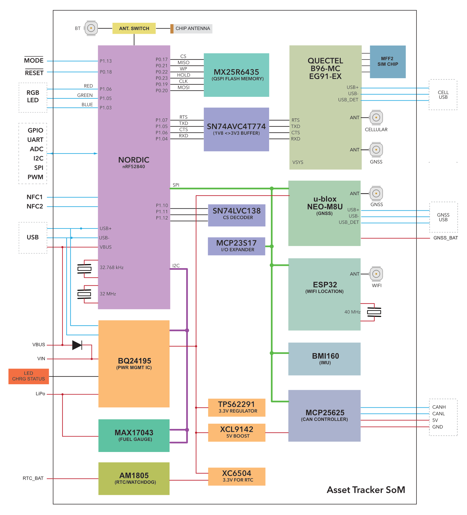
Interfaces
Block diagram
Power
The Tracker SoM can be powered via the VIN (3.9V-17VDC) pin, over USB, or a LiPo battery.
VIN
The input voltage range on VIN pin is 3.9VDC to 17VDC. When powering from the VIN pin alone, make sure that the power supply is rated at 10W (for example 5 VDC at 2 Amp). If the power source is unable to meet this requirement, you'll need connect the LiPo battery as well. An additional bulk capacitance of 470uF to 1000uF should be added to the VIN input when the LiPo Battery is disconnected. The amount of capacitance required will depend on the ability of the power supply to deliver peak currents to the cellular modem.
LiPo
This pin serves two purposes. You can use this pin to connect a LiPo battery (either directly or using a JST connector), or it can be used to connect an external DC power source (and this is where one needs to take extra precautions). When powering it from an external regulated DC source, the recommended input voltage range on this pin is between 3.6V to 4.4VDC. Make sure that the supply can handle currents of at least 3Amp. This is the most efficient way of powering the module since the PMIC bypasses the regulator and supplies power to the module via an internal FET leading to lower quiescent current.
When powered from a LiPo battery alone, the power management IC switches off the internal regulator and supplies power to the system directly from the battery. This reduces the conduction losses and maximizes battery run time. The battery provided with the module is a Lithium-Ion Polymer battery rated at 3.7VDC 1,800mAh. You can substitute this battery with another 3.7V LiPo with higher current rating. Remember to never exceed this voltage rating and always pay attention to the polarity of the connector. A LiPo battery with internal protection circuits is recommended.
Typical current consumption is around 180mA and up to 1.8A transients at 5VDC. In deep sleep mode, the quiescent current is 130uA [this value may change] (powered from the battery alone).
The MAX17043 fuel gauge is only compatible with single cell lithium-ion batteries. The state-of-charge (SoC) values will not be accurate with other battery chemistries.
VBUS
VBUS is connected to the USB detect pin of nRF52840 to enables the USB interface. The recommended input voltage range is between 4.35V to 5.5V DC. It is also connected to the bq24195 PMIC to allow for DPDM, detection of the power capacity of the USB port.
3V3 Pin
This pin is the output of the on-board 3.3V switching regulator that powers the microcontroller and the peripherals. This pin can be used as a 3.3V power source with a max load of 800mA. Unlike the Photon, this pin CANNOT be used as an input to power the module.
RTC_BAT
This is the supply to the real-time clock battery backup. 1.4 to 3.6V.
| Voltage | Typical Current | Peak Current | Unit |
|---|---|---|---|
| 3.0V | 56 | 330 | nA |
| 1.8V | 52 | 290 | nA |
If the RTC battery is not used, connect RTC_BAT to ground.
GNSS_BAT
This is the supply for maintaining the u-blox GNSS ephemeris and almanac data when removing power. This can use the same battery as RTC_BAT, can be a super-capacitor, or can be omitted. 1.5 to 3.6V. Typical current is 15 uA.
If you are not powering GNSS_BAT with a battery or super-capacitor, connect GNSS_BAT to 3V3.
- Saving the ephemeris and almanac data can improve fix/lock time.
- It won't make a difference on completely cold boot, where is no previously saved data.
- It does not make a difference if the GNSS is constantly powered or is using a software power save mode.
PMID
This pin is connected to the PMID pin of the bq24195 PMIC. You should leave this pin unconnected.
Antennas
There are a number of U.FL antenna connectors on the Tracker SoM:
| Label | Purpose |
|---|---|
| GNSS | u-blox GNSS antenna (GPS) |
| CELL | Quectel cellular modem antenna |
| WIFI | Wi-Fi antenna for Wi-Fi geolocation (optional)1 |
| BLE | External Bluetooth (optional)2 |
| GNSS/DIV | Quectel GNSS antenna (optional)1 |
| DIV | LTE cellular receive diversity antenna3 |
1Not supported at this time.
2There is a BLE chip antenna on the module, the external BLE antenna is optional.
3DIV is the connector for the LTE cellular receive diversity antenna (T523 only). A second cellular antenna can be connected to this connector to improve performance when the device will be moving at high speeds. It is only used for LTE Cat 1 connections and is not supported when in 2G or 3G mode. This antenna is not necessary in most cases and is not included in evaluation kits. The T404/T402 do not have this connector as receive diversity is not supported in LTE Cat M1 mode.
There is no U.FL connector for NFC. If you wish to use the NFC tag feature, you'll need to add an antenna or antenna connector on your base board.
- The antenna placement needs to follow some basic rules, as any antenna is sensitive to its environment. Mount the antenna at least 10mm from metal components or surfaces, ideally 20mm for best radiation efficiency, and try to maintain a minimum of three directions free from obstructions to be able to operate effectively.
- Needs tuning with actual product enclosure and all components.
- For the BLE antenna, it is recommended to use a 2.4 GHz single-frequency antenna and not a 2.4 GHz + 5 GHz antenna, so as to avoid large gain at the frequency twice of 2.4 GHz which can cause the second harmonic radiation of 2.4 GHz to exceed standards.
GNSS Antenna
As the GNSS system is receive-only (no transmitter), you can use any GNSS compatible antenna without affecting the certification. Different GNSS systems use different frequencies. Many antennas are tuned to the United States GPS system, however you can also get multi-GNSS antennas that are compatible with other systems. All of these systems offer coverage world-wide.
| System | Owner |
|---|---|
| GPS | United States |
| GLOSNASS | Russia |
| BeiDou | China |
| Galileo | European Space Agency |
Cellular antenna
The Tracker SoM has been certified with the following antenna:
| Antenna | SKU | Details | Links |
|---|---|---|---|
| Particle Cellular Flex Antenna 2G/3G/LTE 4.7dBi, [x1] | ANTCW2EA | Tracker, B-Series, E-Series | Datasheet | Retail Store |
| Band | Frequency (MHz) | Peak Gain | Average Gain |
|---|---|---|---|
| 700/850/900 | 698-960 | 1.42 dBi | -2.80 dB |
| 1700/1800/1900 | 1710-1990 | 3.77 dBi | -1.90 dB |
| 2100 | 1755-2170 | 4.62 dBi | -2.65 dB |
| 2400 | 2400-2500 | 4.71 dBi | -2.10 dB |
| 2600 | 2500-2690 | 4.66 dBi | -2.20 dB |
| Measurement | Value |
|---|---|
| Maximum power | 5W |
| Impedance | 50Ω |
| Size | 97.0 x 21.0 x 0.2 mm |
Particle devices are certified for use only with the designated antenna specified above. The use of alternative antennas with our modules could necessitate a recertification process. To fully understand the potential consequences of using a non-certified antenna, Particle strongly advises seeking consultation with a qualified RF expert.
Wi-Fi Antenna
The Tracker SoM has been certified with the following Wi-Fi antenna. Note: The same external antenna model is used for Wi-Fi and BLE.
| Antenna | SKU | Links |
|---|---|---|
| Particle Wi-Fi Antenna 2.4GHz, [x1] | ANT-FLXV2 | Datasheet | Retail Store |
| Particle Wi-Fi Antenna 2.4GHz, [x50] | ANT-FLXV2-50 | Datasheet |
| Measurement | Value |
|---|---|
| Peak gain | 2.0 dBi |
| Frequency | 2400 - 2500 MHz |
| Impedance | 50Ω |
| Size | 45.1 x 7.4 x 1.0mm |
BLE Antenna
The Tracker SoM includes a built-in chip antenna for BLE with a peak gain of 0 dBi. It can also be used with the following external antenna, which is the same model as the Wi-Fi antenna, above.
| Antenna | SKU | Links |
|---|---|---|
| Particle Wi-Fi Antenna 2.4GHz, [x1] | ANT-FLXV2 | Datasheet | Retail Store |
| Particle Wi-Fi Antenna 2.4GHz, [x50] | ANT-FLXV2-50 | Datasheet |
| Measurement | Value |
|---|---|
| Peak gain | 2.0 dBi |
| Frequency | 2400 - 2500 MHz |
| Impedance | 50Ω |
| Size | 45.1 x 7.4 x 1.0mm |
Peripherals and GPIO
There are 10 exposed GPIO lines labeled A0-A7, TX, and RX. These multi-function pins can be configured for use as GPIO or other interfaces like SPI and I2C.
| Shared Peripherals | Qty | Input(I) / Output(O) |
|---|---|---|
| Digital | 10 (max) | I/O |
| Analog (ADC) | 8 (max) | I |
| UART | 1 | I/O |
| SPI | 1 | I/O |
| I2C | 1 | I/O |
| PWM | 10 (max)1 | O |
| Peripheral Type | Qty | Input(I) / Output(O) |
|---|---|---|
| USB | 1 | I/O |
| NFC Tag | 1 | O |
| CAN Bus | 1 | I/O |
1PWM is divided into three PWM groups. Each group must share the same frequency, but can have different periods.
Note: All GPIO are only rated at 3.3VDC max. CAN bus has a higher voltage rating.
JTAG (SWD)
The AssetTracker SoM exposes the nRF52 SWD interface on the following pins. The Evaluation Board connects these pins to the 2x5 connector used on the Argon and Boron to easily connect the Particle Debugger.
| # | Pin | Function | Connected To | Description |
|---|---|---|---|---|
| 22 | SWDIO | JTAG | nRF52 | nRF52 MCU SWDIO |
| 23 | SWDCLK | JTAG | nRF52 | nRF52 MCU SWDCLK |
| 24 | SWO | JTAG | nRF52 | nRF52 MCU SWO |
This interface can be used to debug your code or reprogram your bootloader, device OS, or the user firmware.
Memory map
nRF52840 flash layout overview
- Bootloader (48KB, @0xF4000)
- User Application
- 256KB @ 0xB4000 (Device OS 3.1 and later)
- 128KB @ 0xD4000 (Device OS 3.0 and earlier)
- System (656KB, @0x30000)
- SoftDevice (192KB)
External SPI flash layout overview (dfu offset: 0x80000000)
- OTA (1500KB, @0x00689000)
- Reserved (420KB, @0x00620000)
- FAC (128KB, @0x00600000)
- Reserved (2MB @0x00400000)
- LittleFS (4MB, @0x00000000)
Pins and connectors
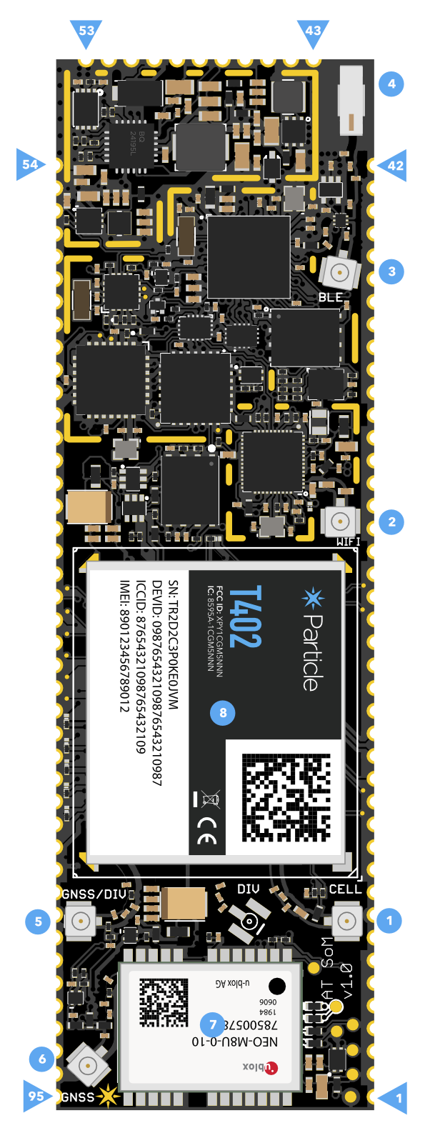
Circular labels are as follows:
| Label | Purpose |
|---|---|
| 1 | Quectel cellular modem antenna |
| 2 | Wi-Fi antenna for Wi-Fi geolocation (optional) |
| 3 | External Bluetooth (optional) |
| 4 | Built-in Bluetooth chip antenna |
| 5 | Quectel GNSS antenna (optional) |
| 6 | u-blox GNSS antenna (GPS) |
| 7 | u-blox Neo M8 GNSS (GPS) |
| 8 | Quectel cellular modem |
SoM Pin description
| # | Pin | Function | Connected To | Description |
|---|---|---|---|---|
| Right Side | ||||
| 1 | GND | POWER | Ground | |
| 2 | GNSS_BAT | POWER IN | GNSS | Battery backup for GNSS |
| 3 | GNSS_RESET | IO | GNSS & IOEX | GNSS hardware reset. Can be controlled by this pin or software. |
| 4 | GNSS_VBUS | USB PWR | GNSS | GNSS USB power. Optional. |
| 5 | GNSS_P | USB D+ | GNSS | GNSS USB interface D+. Optional. |
| 6 | GNSS_N | USB D- | GNSS | GNSS USB interface D-. Optional. |
| 7 | GNSS_PULSE | OUT | GNSS | GNSS time pulse output. Can be used for a GNSS fix LED.2 |
| 8 | GND | POWER | Ground | |
| 9 | NC | Leave unconnected. | ||
| 10 | GND | POWER | Ground | |
| 11 | WIFI_EN | IO | WIFI & IOEX | ESP32 enable. Can be controlled by this pin or software. |
| 12 | WIFI_BOOT | IO | WIFI & IOEX | ESP32 boot mode. Can be controlled by this pin or software. |
| 13 | WIFI_TXD | OUT | WIFI | ESP32 serial TX |
| 14 | WIFI_RXD | IN | WIFI | ESP32 serial TX |
| 15 | CELL_VBUS | USB PWR | CELL | Cellular modem USB power. Optional. |
| 16 | CELL_D+ | USB D+ | CELL | Cellular modem USB interface D+. Optional. |
| 17 | CELL-D- | USB D- | CELL | Cellular modem USB interface D-. Optional. |
| 18 | NC SOM18 | Leave unconnected. | ||
| 19 | NC SOM19 | Leave unconnected. | ||
| 20 | NC SOM20 | Leave unconnected. | ||
| 21 | NC SOM21 | Leave unconnected. | ||
| 22 | SWDIO | JTAG | nRF52 | nRF52 MCU SWDIO |
| 23 | SWDCLK | JTAG | nRF52 | nRF52 MCU SWDCLK |
| 24 | SWO | JTAG | nRF52 | nRF52 MCU SWO |
| 25 | GND | POWER | Ground | |
| 26 | NFC2 | NFC | nRF52 | nRF52 NFC antenna. Supports NFC tag mode only. Optional. |
| 27 | NFC1 | NFC | nRF52 | nRF52 NFC antenna. Supports NFC tag mode only. Optional. |
| 28 | RGB_BLUE | RGB LED | nRF52 | Common anode RGB status LED, blue. Optional. |
| 29 | RGB_GREEN | RGB LED | nRF52 | Common anode RGB status LED, green. Optional. |
| 30 | RGB_RED | RGB LED | nRF52 | Common anode RGB status LED, red. Optional. |
| 31 | GND | POWER | Ground | |
| 32 | MODE | INPUT | nRF52 | External MODE button input, active low. Optional. |
| 33 | RESET | INPUT | nRF52 | External RESET button input, active low. Optional. |
| 34 | NC SOM34 | Leave unconnected. | ||
| 35 | NC SOM35 | Leave unconnected. | ||
| 36 | NC SOM36 | Leave unconnected. | ||
| 37 | NC SOM37 | Leave unconnected. | ||
| 38 | A7 | IO | nRF52 | A7, D7, SS, WKP |
| 39 | A6 | IO | nRF52 | A6, D6, SPI SCK |
| 40 | A5 | IO | nRF52 | A5, D5, SPI MISO |
| 41 | A4 | IO | nRF52 | A4, D4, SPI MOSI |
| 42 | GND | POWER | Ground | |
| Top Side | ||||
| 43 | GND | POWER | Ground | |
| 44 | NC SOM44 | Leave unconnected. | ||
| 45 | 3V3 | POWER OUT | TPS62291 | 3.3V power output. 1000 mA maximum include nRF52 and other peripheral use. |
| 46 | TS | IN | PMIC | Battery temperature sensor |
| 47 | PMID | POWER OUT | PMIC | PMIC power output in OTG mode. |
| 48 | GND | POWER | Ground | |
| 49 | VIN | POWER IN | PMIC | Power input 3.9VDC to 17VDC. |
| 50 | STAT | OUT | PMIC | PMIC charge status. Can be connected to an LED. Active low. Optional. |
| 51 | VBUS | POWER IN | PMIC & nRF52 | nRF52 USB power input. Can be used as a power supply instead of VIN. |
| 52 | GND | POWER | Ground | |
| 53 | LI+ | POWER | PMIC | Connect to Li-Po battery. Can power the device or be recharged by VIN or VBUS. |
| Left Side | ||||
| 54 | GND | POWER | Ground | |
| 55 | A0 | IO | nRF52 | A0, D0, Wire SDA, Thermistor1 |
| 56 | A1 | IO | nRF52 | A1, D1, Wire SCL, User button1 |
| 57 | A2 | IO | nRF52 | A2, D2, Serial1 CTS, GNSS lock indicator1 |
| 58 | A3 | IO | nRF52 | A3, D3, Serial1 RTS, M8 GPIO1 |
| 59 | NC SOM59 | Leave unconnected. | ||
| 60 | NC SOM60 | Leave unconnected. | ||
| 61 | NC SOM61 | Leave unconnected. | ||
| 62 | NC SOM62 | Leave unconnected. | ||
| 63 | AGND | POWER | nRF52 | nRF52 analog ground. Can connect to regular GND. |
| 64 | CAN_N | CAN | CAN | CAN Data- |
| 65 | CAN_P | CAN | CAN | CAN Data+ |
| 66 | CAN_5V | XCL9142F40 | 5V power out, 370 mA maximum. Can be controlled by software. | |
| 67 | GND | POWER | Ground | |
| 68 | MCU-D- | USB D- | nRF52 | MCU USB interface D-. Optional. |
| 69 | MCU_D+ | USB D+ | nRF52 | MCU USB interface D+. Optional. |
| 70 | GND | POWER | Ground | |
| 71 | MCU_RX | IO | nRF52 | Serial RX, GPIO D9, Wire3 SDA |
| 72 | MCU_TX | IO | nRF52 | Serial TX, GPIO D8, Wire3 SCL |
| 73 | RTC_BAT | POWER | AM18X5 | RTC/Watchdog battery +. Connect to GND if not using. |
| 74 | RTC_BTN | IN | AM18X5 | RTC EXTI. Can use as a wake button. |
| 75 | GND | POWER | Ground | |
| 76 | NC SOM76 | Leave unconnected. | ||
| 77 | NC SOM77 | Leave unconnected. | ||
| 78 | NC SOM78 | Leave unconnected. | ||
| 79 | NC SOM79 | Leave unconnected. | ||
| 80 | NC SOM80 | Leave unconnected. | ||
| 81 | NC SOM81 | Leave unconnected. | ||
| 82 | NC SOM82 | Leave unconnected. | ||
| 83 | CELL_GPS_RX | IN | CELL | Cellular modem GPS serial RX data. |
| 84 | CELL_GPS_TX | OUT | CELL | Cellular modem GPS serial TX data. |
| 85 | CELL_RI | OUT | CELL | Cellular modem ring indicator output. |
| 86 | GND | POWER | Ground | |
| 87 | CELL_GPS_RF | RF | CELL | Cellular modem GPS antenna. Optional. |
| 88 | GND | POWER | Ground | |
| 89 | GND | POWER | Ground | |
| 90 | GNSS_BOOT | GNSS | u-blox GNSS boot mode | |
| 91 | GNSS_ANT_PWR | GNSS | u-blox GNSS antenna power | |
| 92 | GNSS_LNA_EN | GNSS | u-blox GNSS LNA enable or antenna switch | |
| 93 | GND | POWER | Ground | |
| 94 | GNSS_RF | GNSS | GNSS antenna. | |
| 95 | GND | POWER | Ground |
Note: All GPIO, ADC, and peripherals such as I2C, Serial, and SPI are 3.3V maximum and are not 5V tolerant.
Pin numbers match the triangular numbers in the graphic above.
1Pin usage on the Tracker One.
2The GNSS_PULSE pin can be used for a hardware GPS lock indicator, however the Tracker One controls the GNSS Lock indicator in software and connects the LED to pin A2.
nRF52 pin assignments
| SoM Pin | GPIO | Analog | Other | PWM | nRF Pin |
|---|---|---|---|---|---|
| 55 | D0 | A0 | Wire SDA1 | Group 0 | P0.03 |
| 56 | D1 | A1 | Wire SCL1 | Group 0 | P0.02 |
| 57 | D2 | A2 | Serial1 CTS | Group 0 | P0.28 |
| 58 | D3 | A3 | Serial1 RTS | Group 0 | P0.30 |
| 41 | D4 | A4 | SPI MOSI | Group 1 | P0.31 |
| 40 | D5 | A5 | SPI MISO | Group 1 | P0.29 |
| 39 | D6 | A6 | SPI SCK | Group 1 | P0.04 |
| 38 | D7 | A7 | SPI SS, WKP | Group 1 | P0.05 |
| 72 | D8 | Serial1 TX, Wire3 SCL | Group 2 | P0.06 | |
| 71 | D9 | Serial1 RX, Wire3 SDA | Group 2 | P0.08 |
1Pull-up resistors are not included. When using as an I2C port, external pull-up resistors are required.
System peripheral GPIO
| Name | Description | Location |
|---|---|---|
| BTN | MODE Button | P1.13 |
| PMIC_INT | PMIC Interrupt | P0.26 |
| LOW_BAT_UC | Fuel Gauge Interrupt | IOEX 0.0 |
| RTC_INT | Real-time clock Interrupt | P0.27 |
| BGRST | Cellular module reset | P0.07 |
| BGPWR | Cellular module power | P0.08 |
| BGVINT | Cellular power on detect | P1.14 |
| BGDTR | Cellular module DTR | IOEX 1.5 |
| CAN_INT | CAN interrupt | P1.09 |
| CAN_RST | CAN reset | IOEX 1.6 |
| CAN_PWR | 5V boost converter enable | IOEX 1.7 |
| CAN_STBY | CAN standby mode | IOEX 0.2 |
| CAN_RTS0 | CAB RTS0 | IOEX 1.4 |
| CAN_RTS1 | CAN RTS1 | IOEX 1.2 |
| CAN_RTS2 | CAN RTS2 | IOEX 1.3 |
| SEN_INT | IMU interrupt | P1.07 |
| ANT_SW1 | BLE antenna switch | P1.15 |
| GPS_PWR | u-blox GNSS power | IOEX 0.6 |
| GPS_INT | u-blox GNSS interrupt | IOEX 0.7 |
| GPS_BOOT | u-blox GNSS boot mode | IOEX 1.0 |
| GPS_RST | u-blox GNSS reset | IOEX 1.1 |
| WIFI_EN | ESP32 enable | IOEX 0.3 |
| WIFI_INT | ESP32 interrupt | IOEX 0.4 |
| WIFI_BOOT | ESP32 boot mode | IOEX 0.5 |
Status LED
The Tracker SoM does not have an on-module RGB system status LED. We have provided its individual control pins for you to connect an LED of your liking. This will allow greater flexibility in the end design of your products.
Device OS assumes a common anode RGB LED. One common LED that meets the requirements is the Cree CLMVC-FKA-CL1D1L71BB7C3C3 which is inexpensive and easily procured. You need to add three current limiting resistors. With this LED, we typically use 1K ohm current limiting resistors. These are much larger than necessary. They make the LED less blinding but still provide sufficient current to light the LEDs. If you want maximum brightness you should use the calculated values - 33 ohm on red, and 66 ohm on green and blue.
A detailed explanation of different color codes of the RGB system LED can be found here.
Technical specifications
Absolute maximum ratings
| Parameter | Symbol | Min | Typ | Max | Unit |
|---|---|---|---|---|---|
| Supply | |||||
| Supply Input Voltage | VIN | -2.0 | +22.0 | V | |
| Supply Input Current | IIN-MAX-L | 1.5 | A | ||
| VBUS USB supply voltage | VUSB | -0.3 | +5.8 | V | |
| Supply Output Voltage | VIN | +4.8 | V | ||
| Supply Output Voltage | V3V3 | +3.3 | V | ||
| Supply Output Current | I3V3-MAX-L | 800 | mA | ||
| LiPo Battery Voltage | VLiPo | -0.5 | +6.0 | V | |
| CAN Supply Voltage | 5 | V | |||
| CAN Supply Current | 370 | mA | |||
| I/O pin voltage | |||||
| VI/O | IO | -0.3 | +3.6 | V | |
| NFC antenna pin current | |||||
| INFC1/2 | NFC1/NFC2 | 80 | mA | ||
| Radio | |||||
| BT RF input level (52840) | 10 | dBm | |||
| Environmental | |||||
| Storage temperature | -40 | +85 | °C | ||
| ESD Susceptibility HBM (Human Body Mode) | VESD | 2 | kV |
Stresses beyond those listed under absolute maximum ratings may cause permanent damage to the device. These are stress ratings only, and functional operation of the device at these or any other conditions beyond those indicated under recommended operating conditions is not implied. Exposure to absolute-maximum-rated conditions for extended periods may affect device reliability.
Recommended operating conditions
| Parameter | Symbol | Min | Typ | Max | Unit |
|---|---|---|---|---|---|
| Supply voltages | |||||
| Supply Input Voltage | VIN | 3.9 | 17.0 | V | |
| VBUS USB supply voltage | VUSB | 4.35 | 5.0 | 5.5 | V |
| LiPo Battery Voltage | VLiPo | 3.6 | 4.3 | V | |
| Environmental | |||||
| Normal operating temperature1 | -20 | +25 | +75 | °C | |
| Extended operating temperature2 | -40 | +85 | °C | ||
| Humidity Range Non condensing, relative humidity | 95 | % |
Notes:
1 Normal operating temperature range (fully functional and meet 3GPP specifications).
2 Extended operating temperature range (RF performance may be affected outside normal operating range, though module is fully functional)
Power consumption (T404/T402)
| Parameter | Symbol | Min | Typ | Peak | Unit |
|---|---|---|---|---|---|
| Operating Current (uC on, peripherals and radio disabled) | Iidle | 3.35 | 3.38 | 4.39 | mA |
| Operating Current (uC on, cellular on but not connected) | Icell_idle | 21.3 | 277 | mA | |
| Operating Current (uC on, cellular connecting to tower) | Icell_conn_twr | 16.8 | 56.7 | 329 | mA |
| Operating Current (uC on, cellular connecting to cloud) | Icell_conn_cloud | 19.1 | 53.3 | 292 | mA |
| Operating Current (uC on, cellular connected but idle) | Icell_cloud_idle | 19.2 | 21.2 | 97.1 | mA |
| Operating Current (uC on, cellular connected and transmitting) | Icell_cloud_tx | 19.5 | 63.6 | 280 | mA |
| STOP mode sleep, GPIO wake-up | Istop_gpio | 556 | 806 | 1170 | uA |
| STOP mode sleep, analog wake-up | Istop_analog | 588 | 831 | 1230 | uA |
| STOP mode sleep, RTC wake-up | Istop_intrtc | 593 | 835 | 1240 | uA |
| STOP mode sleep, BLE wake-up, advertising | Istop_ble_adv | 858 | 2330 | uA | |
| STOP mode sleep, BLE wake-up, connected | Istop_ble_conn | 875 | 1600 | uA | |
| STOP mode sleep, serial wake-up | Istop_usart | 577 | 798 | 1210 | uA |
| STOP mode sleep, cellular wake-up | Istop_cell | 7.66 | 17.2 | 90.1 | mA |
| STOP mode sleep, IMU wake-up | Istop_imu | 548 | 834 | 1250 | uA |
| STOP mode sleep, CAN wake-up | Istop_can | 605 | 817 | 1210 | uA |
| STOP mode sleep, GPS wake-up | Istop_gps | 23.7 | 31.1 | 46.3 | mA |
| ULP mode sleep, GPIO wake-up | Iulp_gpio | 114 | 479 | uA | |
| ULP mode sleep, analog wake-up | Iulp_analog | 117 | 508 | uA | |
| ULP mode sleep, RTC wake-up | Iulp_intrtc | 114 | 509 | uA | |
| ULP mode sleep, BLE wake-up, advertising | Iulp_ble_adv | 186 | 2200 | uA | |
| ULP mode sleep, BLE wake-up, connected | Iulp_ble_conn | 203 | 1070 | uA | |
| ULP mode sleep, serial wake-up | Iulp_usart | 287 | 530 | 934 | uA |
| ULP mode sleep, cellular wake-up | Iulp_cell | 3.06 | 16.9 | 83.4 | mA |
| ULP mode sleep, IMU wake-up | Iimu_imu | 175 | 616 | uA | |
| ULP mode sleep, CAN wake-up | Ican_can | 142 | 528 | uA | |
| ULP mode sleep, GPS wake-up | Iulp_gps | 23.6 | 30.9 | 45.7 | mA |
| HIBERNATE mode sleep, GPIO wake-up | Ihib_gpio | 103 | 503 | uA | |
| HIBERNATE mode sleep, analog wake-up | Ihib_analog | 100 | 493 | uA | |
| HIBERNATE mode sleep, external RTC wake-up | Ihib_extrtc | 94.3 | 590 | uA | |
| HIBERNATE mode sleep, IMU wake-up | Ihib_imu | 151 | 590 | uA | |
| HIBERNATE mode sleep, CAN wake-up | Ihib_can | 121 | 477 | uA |
1The min, and particularly peak, values may consist of very short transients. The typical (typ) values are the best indicator of overall power consumption over time. The peak values indicate the absolute minimum capacity of the power supply necessary, not overall consumption.
Current measurements taken at 3.6V via the battery input. For more information about measuring power usage, see power measurement.
Power consumption (t524/t523)
| Parameter | Symbol | Min | Typ | Peak | Unit |
|---|---|---|---|---|---|
| Operating Current (uC on, peripherals and radio disabled) | Iidle | 3.22 | 3.24 | 3.26 | mA |
| Operating Current (uC on, cellular on but not connected) | Icell_idle | 18.9 | 22.0 | 136 | mA |
| Operating Current (uC on, cellular connecting to tower) | Icell_conn_twr | 35.5 | 106 | 726 | mA |
| Operating Current (uC on, cellular connecting to cloud) | Icell_conn_cloud | 38.0 | 137 | 553 | mA |
| Operating Current (uC on, cellular connected but idle) | Icell_cloud_idle | 19.2 | 21.2 | 97.1 | mA |
| Operating Current (uC on, cellular connected and transmitting) | Icell_cloud_tx | 117 | 145 | 787 | mA |
| STOP mode sleep, GPIO wake-up | Istop_gpio | 625 | 872 | 1270 | uA |
| STOP mode sleep, analog wake-up | Istop_analog | 655 | 853 | 1210 | uA |
| STOP mode sleep, RTC wake-up | Istop_intrtc | 632 | 873 | 1260 | uA |
| STOP mode sleep, BLE wake-up, advertising | Istop_ble_adv | 919 | 2700 | uA | |
| STOP mode sleep, BLE wake-up, connected | Istop_ble_conn | 421 | 901 | 1680 | uA |
| STOP mode sleep, serial wake-up | Istop_usart | 613 | 840 | 1240 | uA |
| STOP mode sleep, cellular wake-up | Istop_cell | 19.2 | 21.5 | 149 | mA |
| STOP mode sleep, IMU wake-up | Istop_imu | 584 | 858 | 1250 | uA |
| STOP mode sleep, CAN wake-up | Istop_can | 622 | 869 | 1280 | uA |
| STOP mode sleep, GPS wake-up | Istop_gps | 23.8 | 30.8 | 44.7 | mA |
| ULP mode sleep, GPIO wake-up | Iulp_gpio | 130 | 139 | 540 | uA |
| ULP mode sleep, analog wake-up | Iulp_analog | 132 | 140 | 542 | uA |
| ULP mode sleep, RTC wake-up | Iulp_intrtc | 131 | 139 | 531 | uA |
| ULP mode sleep, BLE wake-up, advertising | Iulp_ble_adv | 132 | 214 | 2240 | uA |
| ULP mode sleep, BLE wake-up, connected | Iulp_ble_conn | 230 | 1110 | uA | |
| ULP mode sleep, serial wake-up | Iulp_usart | 366 | 564 | 933 | uA |
| ULP mode sleep, cellular wake-up | Iulp_cell | 18.9 | 21.7 | 210 | mA |
| ULP mode sleep, IMU wake-up | Iimu_imu | 172 | 580 | uA | |
| ULP mode sleep, CAN wake-up | Ican_can | 162 | 513 | uA | |
| ULP mode sleep, GPS wake-up | Iulp_gps | 23.1 | 30.2 | 44.6 | mA |
| HIBERNATE mode sleep, GPIO wake-up | Ihib_gpio | 111 | 474 | uA | |
| HIBERNATE mode sleep, analog wake-up | Ihib_analog | 114 | 521 | uA | |
| HIBERNATE mode sleep, external RTC wake-up | Ihib_extrtc | 111 | 478 | uA | |
| HIBERNATE mode sleep, IMU wake-up | Ihib_imu | 144 | 580 | uA | |
| HIBERNATE mode sleep, CAN wake-up | Ihib_can | 8.76 | 133 | 386 | uA |
1The min, and particularly peak, values may consist of very short transients. The typical (typ) values are the best indicator of overall power consumption over time. The peak values indicate the absolute minimum capacity of the power supply necessary, not overall consumption.
Current measurements taken at 3.6V via the battery input. For more information about measuring power usage, see power measurement.
GNSS specifications
- u-blox NEO-M8U untethered dead reckoning module including 3D inertial sensors
- SPI Interface
- Supports GPS L1C/A, Galileo E1B/C
| Parameter | Specification |
|---|---|
| Dynamics operational limit1 | ≤ 4g |
| Altitude operational limit1 | 50000 m |
| Velocity operational limit1 | 500 m/s |
| Velocity accuracy2 | 0.5 m/s |
| Heading accuracy2 | 1 degree |
| Max navigation update rate3 | 30 Hz |
| Max navigation latency3 | < 10 ms |
| Parameter | GPS | Galileo | |
|---|---|---|---|
| Time-To-First Fix5 | Cold start | 30s | 57s |
| Hot start | 1.5s | 1.5s | |
| Aided start6 | 3s | 7s | |
| Sensitivity 78 | Tracking & Navigation | -160 dBm | -154 dBm |
| Reacquisiton | -159 dBm | -152 dBm | |
| Cold Start | -147 dBm | -133 dBm | |
| Hot Start | -156 dBm | -151 dBm | |
| Horizontal positioning accuracy | Autonomous 9 | TBC10 | |
| With SBAS11 | 1.5m | - | |
| Altitude accuracy | With SBAS12 | 3.0m | - |
1 Configured for Airborne < 4g platform
2 50% at 30 m/s
3 High navigation rate mode
5 All satellites at -130 dBm, except Galileo at -127 dBm
6 Dependent on aiding data connection speed and latency
7 Demonstrated with a good external LNA
8 Configured min. CNO of 6 dB/Hz, limited by FW with min. CNO of 20 dB/Hz for best performance
9 CEP, 50%, 24 hours static, -130 dBm, > 6 SVs
10 To be confirmed when Galileo reaches full operational capability
11 CEP, 50%, 24 hours static, -130 dBm, > 6 SVs
12 CEP, 50%, 24 hours static, -130 dBm, > 6 SVs
GNSS GPIO:
| Name | Description | Location |
|---|---|---|
| GPS_PWR | u-blox GNSS power | IOEX 0.6 |
| GPS_INT | u-blox GNSS interrupt | IOEX 0.7 |
| GPS_BOOT | u-blox GNSS boot mode | IOEX 1.0 |
| GPS_RST | u-blox GNSS reset | IOEX 1.1 |
| GPS_CS | CAN SPI Chip Select | CS Decoder 4 |
CAN specifications
- Microchip MCP25625 CAN Controller with Integrated Transceiver
- SPI Interface
- Implements CAN2.0B (ISO11898-1)
- Implements ISO-11898-2 and ISO-11898-5 standard physical layer requirements
- Up to 1 Mb/sec operation
- 3 transmit buffers with prioritization and abort features
- 2 receive buffers
- 6 filters and 2 masks with optional filtering on the first 2 data bytes
- CAN bus pins are disconnected when device is unpowered
- High-ESD protection on CANH and CANL, meets IEC61000-4-2 up to ±8 kV
- Very low standby current, 10 uA, typical
- 5V step-up converter (XC9142F50CER), 370 mA maximum
- CAN terminator resistor is not included
CAN GPIO:
| Name | Description | Location |
|---|---|---|
| CAN_INT | CAN interrupt | P1.09 |
| CAN_RST | CAN reset (LOW = reset for 100 milliseconds) | IOEX 1.6 |
| CAN_PWR | 5V boost converter enable (HIGH = on) | IOEX 1.7 |
| CAN_STBY | CAN standby mode (HIGH = standby) | IOEX 0.2 |
| CAN_RTS0 | CAB RTS0 | IOEX 1.4 |
| CAN_RTS1 | CAN RTS1 | IOEX 1.2 |
| CAN_RTS2 | CAN RTS2 | IOEX 1.3 |
| CAN_CS | CAN SPI Chip Select | CS Decoder 7 |
CANH, CANL Absolute Maximum Ratings:
| Parameter | Maximum |
|---|---|
| DC Voltage at CANH, CANL | -58V to +58V |
| Transient Voltage on CANH, CANL (ISO-7637) | -150V to +100V |
| ESD Protection on CANH and CANL Pins (IEC 61000-4-2) | ±8 kV |
| ESD Protection on CANH and CANL Pins (IEC 801; Human Body Model) | ±8 kV |
CAN Transceiver Characteristics
| Parameter | Symbol | Min | Typ | Max | Unit | Conditions |
|---|---|---|---|---|---|---|
| Supply Input Voltage | VDDA | 5.0 | V | |||
| Supply Current | IDD | 5 | 10 | mA | Recessive; VTXD = VDDA | |
| 45 | 70 | mA | Dominant; VTXD = 0V | |||
| Standby Current | IDDS | 5 | 15 | µA | Includes IIO | |
| CANH, CANL Recessive Bus Output Voltage | VO(R) | 2.0 | 2.5 | 3.0 | V | VTXD = VDDA |
| CANH, CANL Bus Output Voltage in Standby | VO(S) | -0.1 | 0.0 | +0.1 | V | STBY = VTXD = VDDA; No load |
| Recessive Output Current | IO(R) | -5 | +5 | mA | -24V < VCAN < +24V | |
| CANH: Dominant Output Voltage | VO(D) | 2.75 | 3.5 | 4.5 | V | TXD =0; RL = 50 to 65Ω |
| CANL: Dominant Output Voltage | VO(D) | 0.5 | 1.5 | 2.25 | V | RL = 50 to 65Ω |
| Dominant: Differential Output Voltage | VO(DIFF) | 1.5 | 2.0 | 3.0 | V | TXD = VSS; RL =50 to 65Ω |
| Recessive: Differential Output Voltage | -120 | 0 | 12 | mV | TXD = VDDA; RL =50 to 65Ω | |
| -500 | 0 | 50 | mV | TXD = VDDA; No load | ||
| CANH: Short-Circuit Output Current | IO(SC) | -120 | 85 | mA | VTXD = VSS; VCANH = 0V; CANL: floating | |
| CANL: Short-Circuit Output Current | 75 | 120 | mA | VTXD = VSS; VCANL = 18V; CANH: floating | ||
| Recessive Differential Input Voltage | VDIFF(R)(I) | -1.0 | +0.5 | V | Normal mode; -12V < V(CANH, CANL) < +12V | |
| -1.0 | +0.4 | V | Standby mode; -12V < V(CANH, CANL) < +12V | |||
| Dominant Differential Input Voltage | VDIFF(D)(I) | 0.9 | 5.0 | V | Normal mode; -12V < V(CANH, CANL) < +12V | |
| 1.0 | 5.0 | V | Standby mode; -12V < V(CANH, CANL) < +12V |
Other components
IMU (inertial measurement unit)
- Bosch Sensortec BMI160
- SPI Interface connected to SPI1 (MISO1, MOSI1, SCK1)
- Chip Select: SEN_CS (CS Decoder 2)
Can wake nRF52 MCU on movement (SEN_INT1)
16 bit digital, triaxial accelerometer and triaxial gyroscope
- Very low power consumption: typically 925 μA with accelerometer and gyroscope in full operation
- Allocatable FIFO buffer of 1024 bytes (capable of handling external sensor data)
- Hardware sensor time-stamps for accurate sensor data fusion
- Integrated interrupts for enhanced autonomous motion detection
PMIC
- Texas Instruments bq24195
- I2C interface (Wire1 address 0x6B)
Can interrupt nRF52 MCU on charge status and fault
Handles switching between USB, VIN, and battery power
- LiPo battery charger
- Charge safety timer, thermal regulation, and thermal shutdown
Fuel gauge
- MAX17043
- I2C interface (Wire1 address 0x36)
Can interrupt nRF52 MCU on low battery
Fuel-gauge system for single cell lithium-ion (Li+) batteries
- Precision voltage measurement ±12.5mV Accuracy to 5V
- Accurate relative capacity (RSOC) Ccalculated from ModelGauge algorithm
- No offset accumulation on measurement
- No full-to-empty battery relearning necessary
RTC/Watchdog
- Ambiq Micro AM18X5 Real-Time Clock with Power Management
- 55 nA power consumption
- Crystal oscillator
- I2C interface (Wire1 address 0x68)
- Can wake MCU from hibernate (SLEEP_MODE_DEEP) at a specific time using
RTC_INT. - Programmable hardware watchdog
- RTC powered by XC6504 ultra-low consumption regulator so the main TPS62291 can be shut down from RTC
Wi-Fi Geolocation
The Wi-Fi module is intended for Wi-Fi geolocation only. It cannot be used as a network interface instead of using cellular.
- ESP32-D2WD
- SPI Interface
- Connected to SPI1 (MISO1, MOSI1, SCK1)
- Chip Select: WIFI_CS (CS Decoder 3)
- Interrupt: ESP32 IO4 is connected to MCP23S17 I/0 Expander GPA4.
The SoM connector has several pins dedicated to Wi-Fi:
| # | Pin | Function | Connected To | Description |
|---|---|---|---|---|
| 11 | WIFI_EN | IO | WIFI & IOEX | ESP32 enable. Can be controlled by this pin or software. |
| 12 | WIFI_BOOT | IO | WIFI & IOEX | ESP32 boot mode. Can be controlled by this pin or software. |
| 13 | WIFI_TXD | OUT | WIFI | ESP32 serial TX |
| 14 | WIFI_RXD | IN | WIFI | ESP32 serial TX |
The WIFI_EN pin turns on the Wi-Fi module. LOW=Off, HIGH=On. The default is off (with a 100K weak pull-down). It can be turned on from Pin 11 on the SoM connection, or in software from the MCP23S17 I/0 Expander 0.3.
The WIFI_BOOT pin enables programming mode.
3.3V Regulator
- Texas Instruments TPS62291
- 1.0A at 3.3V
- Powers nRF52840 MCU and ESP32 Wi-Fi module
- Can be used by your base board to power 3.3V components
- 3.3V supply can be powered down from the RTC/Watchdog
Radio specifications
nRF52840
- Bluetooth® 5, 2.4 GHz
- 95 dBm sensitivity in 1 Mbps Bluetooth® low energy mode
- 103 dBm sensitivity in 125 kbps Bluetooth® low energy mode (long range)
- 20 to +8 dBm TX power, configurable in 4 dB steps
4G LTE cellular characteristics for EG91-EX
| Parameter | Value |
|---|---|
| Protocol stack | 3GPP Release 13 |
| RAT | LTE Cat 1 |
| LTE FDD Bands | Band 28 (700 MHz) |
| Band 20 (800 MHz) | |
| Band 8 (900 MHz) | |
| Band 3 (1800 MHz) | |
| Band 1 (2100 MHz) | |
| Band 7 (2600 MHz) | |
| WCDMA Bands | Band 8 (900 MHz) |
| Band 1 (2100) | |
| GSM Bands | EGSM900 (900 MHz) |
| DCS1800 (1800 MHz) | |
| Power class | Class 4 (33dBm ± 2dB) for EGSM900 |
| Class 1 (30dBm ± 2dB) for DCS1800 | |
| Class E2 (27dBm ± 3dB) for EGSM900 8-PSK | |
| Class E2 (26dBm ± 3dB) for DCS1800 8-PSK | |
| Class 3 (24dBm ± 3dB) for WCDMA bands | |
| Class 3 (23dBm ± 2dB) for LTE FDD bands |
4G LTE cellular characteristics for BG96-MC
| Parameter | Value |
|---|---|
| Protocol stack | 3GPP Release 13 |
| RAT | LTE Cat M1 |
| LTE FDD Bands | Band 12 (700 MHz) |
| Band 12 (700 MHz) | |
| Band 13 (700 MHz) | |
| Band 28 (700 MHz) | |
| Band 20 (800 MHz) | |
| Band 5 (850 MHz) | |
| Band 18 (850 MHz) | |
| Band 19 (850 MHz) | |
| Band 26 (850 MHz) | |
| Band 8 (900 MHz) | |
| Band 4 (1700 MHz) | |
| Band 3 (1800 MHz) | |
| Band 2 (1900 MHz) | |
| Band 25 (1900 MHz) | |
| Band 1 (2100 MHz) |
ESP32
Espressif Systems ESP32 for Wi-Fi geolocation:
| Feature | Description |
|---|---|
| WLAN Standards | IEEE 802.11b/g/n |
| Antenna Port | Single Antenna |
| Frequency Band | 2412 to 2484 MHz |
I/O characteristics
These specifications are based on the nRF52840 datasheet.
| Symbol | Parameter | Min | Typ | Max | Unit |
|---|---|---|---|---|---|
| VIH | Input high voltage | 0.7 xVDD | VDD | V | |
| VIL | Input low voltage | VSS | 0.3 xVDD | V | |
| VOH,SD | Output high voltage, standard drive, 0.5 mA, VDD ≥1.7 | VDD - 0.4 | VDD | V | |
| VOH,HDH | Output high voltage, high drive, 5 mA, VDD >= 2.7 V | VDD - 0.4 | VDD | V | |
| VOH,HDL | Output high voltage, high drive, 3 mA, VDD >= 1.7 V | VDD - 0.4 | VDD | V | |
| VOL,SD | Output low voltage, standard drive, 0.5 mA, VDD ≥1.7 | VSS | VSS + 0.4 | V | |
| VOL,HDH | Output low voltage, high drive, 5 mA, VDD >= 2.7 V | VSS | VSS + 0.4 | V | |
| VOL,HDL | Output low voltage, high drive,3 mA, VDD >= 1.7 V | VSS | VSS + 0.4 | V | |
| IOL,SD | Current at VSS+0.4 V, output set low, standard drive, VDD≥1.7 | 1 | 2 | 4 | mA |
| IOL,HDH | Current at VSS+0.4 V, output set low, high drive, VDD >= 2.7V | 6 | 10 | 15 | mA |
| IOL,HDL | Current at VSS+0.4 V, output set low, high drive, VDD >= 1.7V | 3 | mA | ||
| IOH,SD | Current at VDD-0.4 V, output set high, standard drive, VDD≥1.7 | 1 | 2 | 4 | mA |
| IOH,HDH | Current at VDD-0.4 V, output set high, high drive, VDD >= 2.7V | 6 | 9 | 14 | mA |
| IOH,HDL | Current at VDD-0.4 V, output set high, high drive, VDD >= 1.7V | 3 | mA | ||
| tRF,15pF | Rise/fall time, standard drivemode, 10-90%, 15 pF load1 | 9 | ns | ||
| tRF,25pF | Rise/fall time, standard drive mode, 10-90%, 25 pF load1 | 13 | ns | ||
| tRF,50pF | Rise/fall time, standard drive mode, 10-90%, 50 pF load1 | 25 | ns | ||
| tHRF,15pF | Rise/Fall time, high drive mode, 10-90%, 15 pF load1 | 4 | ns | ||
| tHRF,25pF | Rise/Fall time, high drive mode, 10-90%, 25 pF load1 | 5 | ns | ||
| tHRF,50pF | Rise/Fall time, high drive mode, 10-90%, 50 pF load1 | 8 | ns | ||
| RPU | Pull-up resistance | 11 | 13 | 16 | kΩ |
| RPD | Pull-down resistance | 11 | 13 | 16 | kΩ |
| CPAD | Pad capacitance | 3 | pF | ||
| CPAD_NFC | Pad capacitance on NFC pads | 4 | pF | ||
| INFC_LEAK | Leakage current between NFC pads when driven to different states | 1 | 10 | μA |
Rise and fall times based on simulations
GPIO default to standard drive (2mA) but can be reconfigured to high drive (9mA) in Device OS 2.0.0 and later using the
pinSetDriveStrength()function.
Mechanical specifications
Dimensions and weight
| Parameter | Value | Units |
|---|---|---|
| Width | 28 | mm |
| Length | 93 | mm |
| Thickness | 4 | mm |
| Weight | g |
Weight will be provided at a later date.
Mechanical drawing
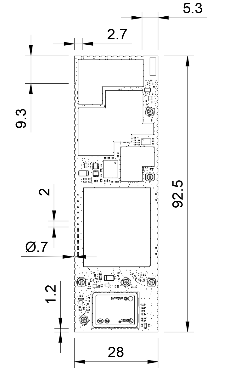
Dimensions are in millimeters.
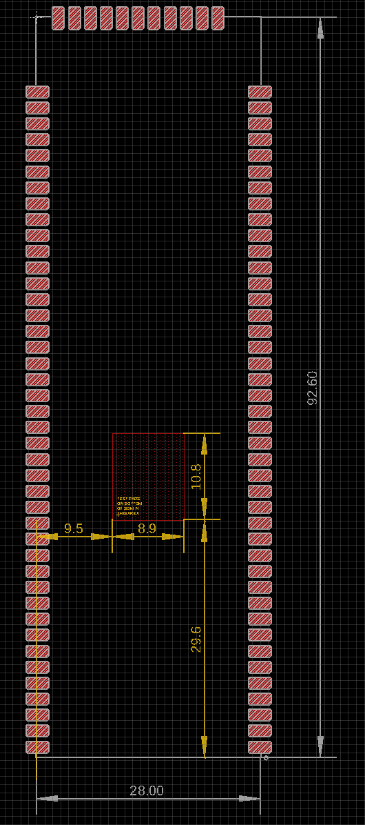
Footprint
A footprint, symbol, and device for Eagle CAD can be found in Particle-devices.lbr in the hardware-libraries Github.
You can place traces and vias under the Tracker SoM module, except in the tRestrict area (red with dots) in the footprint. There are exposed manufacturing test pads on the bottom of the SoM in this rectangles, and you should avoid traces on the top layer and visa in this area.
3D models
3D models of the Tracker SoM module are available in the hardware-libraries Github in formats including step, iges, and stl.
The 3D models are the same for the T404 and T402. They are also the same for the T524 and T523, as the only changes are the SIM card, which is not visible.
Schematics
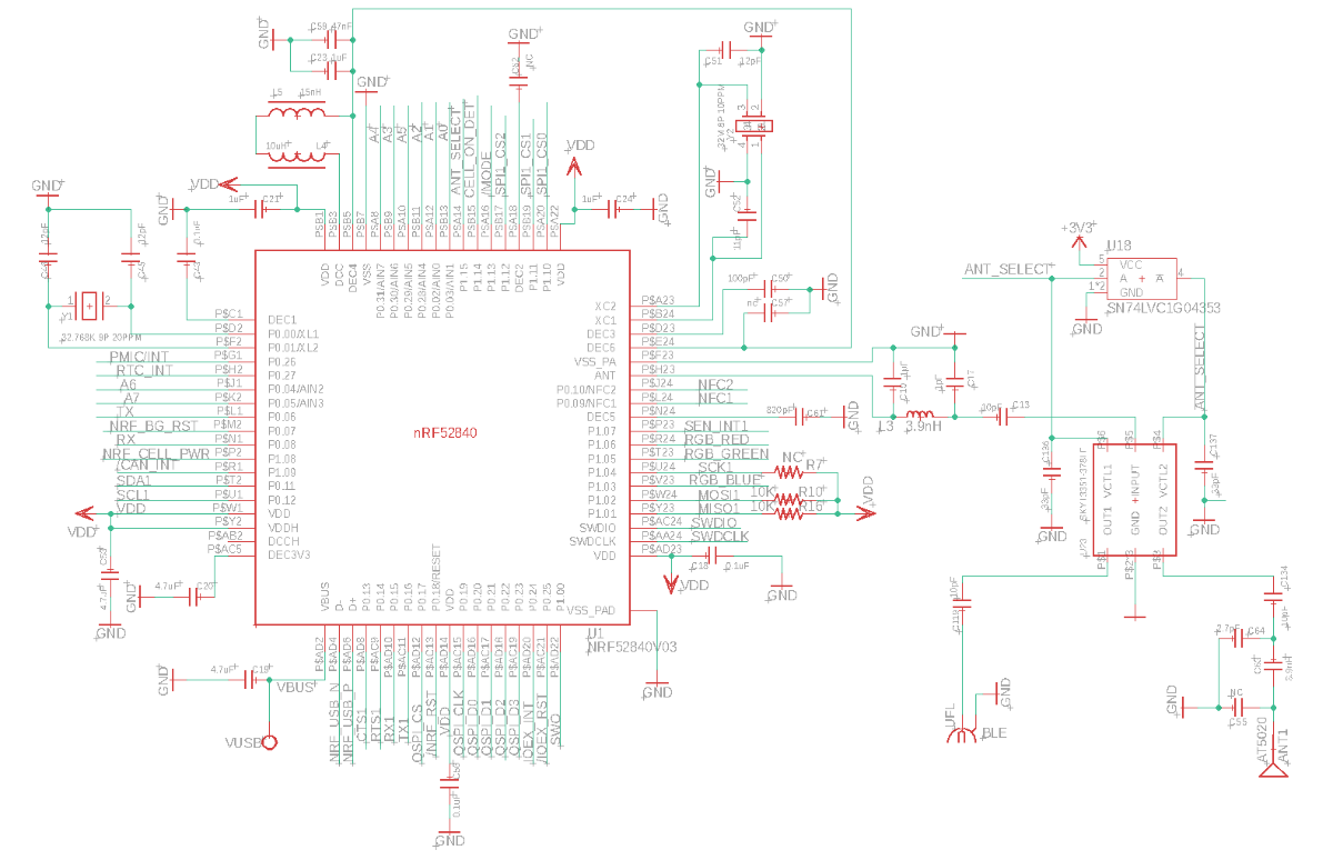
MCU
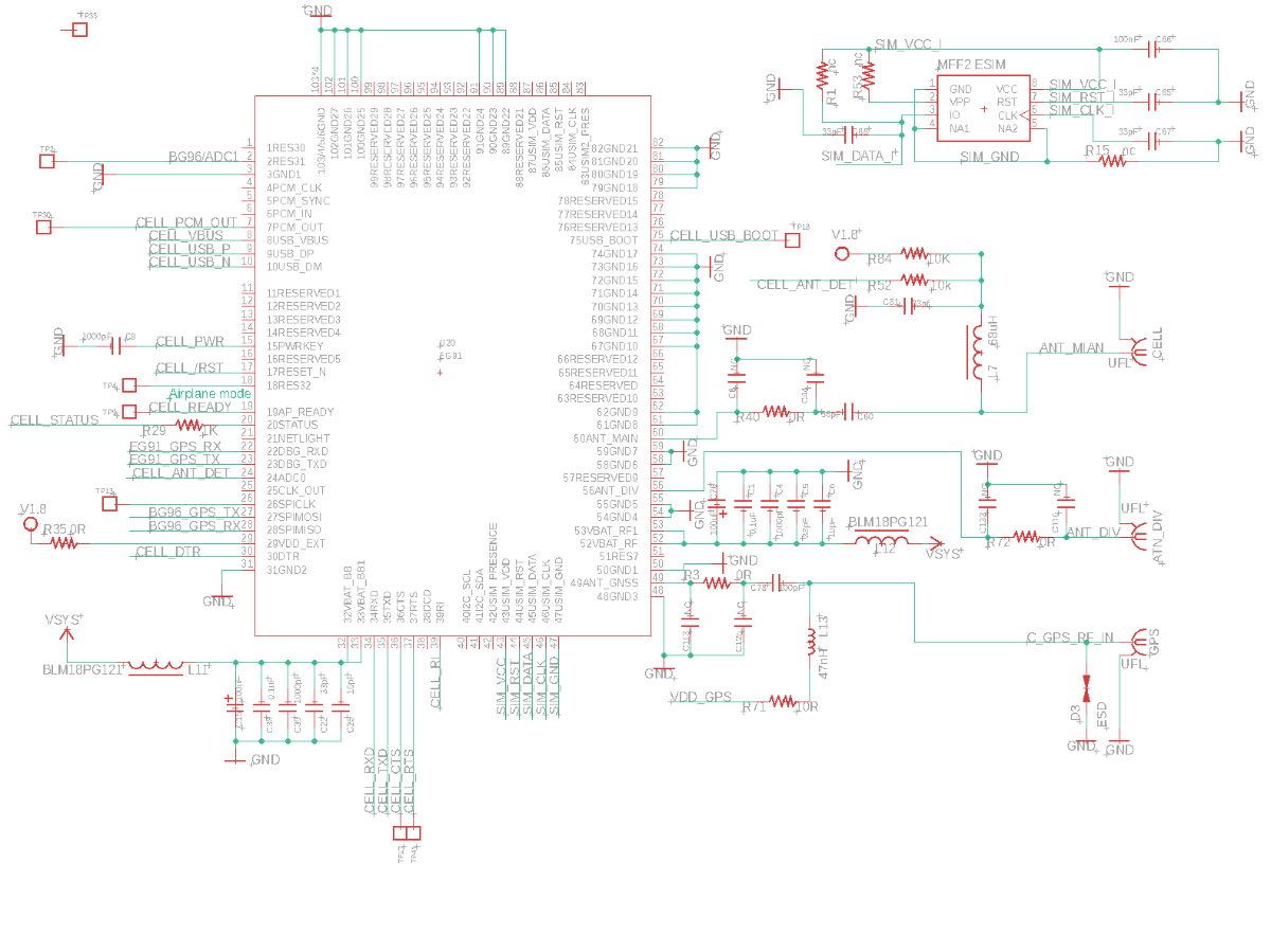
Cellular
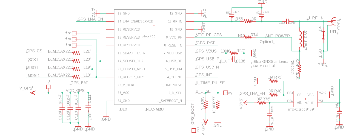
GNSS
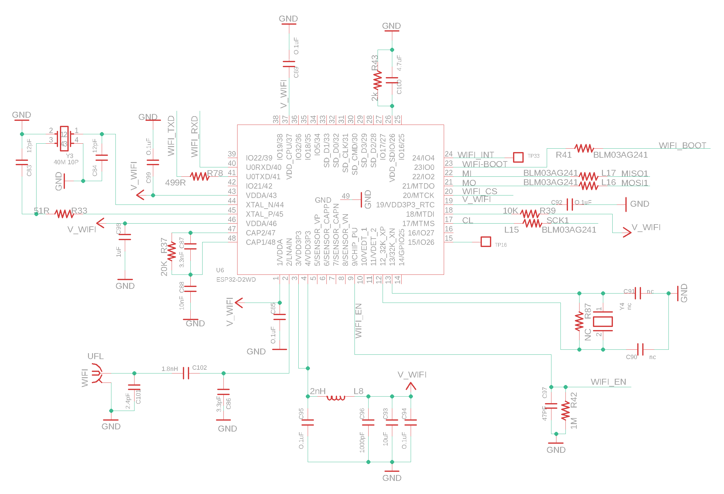
Wi-Fi
CAN
User I/O
PMIC
Fuel gauge
Cell control
I/O expander
QSPI Flash
RTC/Watchdog
IMU
3V3 Regulator
Layout considerations
For information on production soldering, stencils, and layout, see AN036 LCC Module SMT.
Assembly
Water soluble flux
Water soluble flux should not be used with the Tracker SoM module. There are components within the Tracker SoM that are moisture-sensitive, and wash water can get trapped under the RF shields, causing damage.
Use no-clean flux instead.
Conformal coatings
We do not recommend using a conformal coating on the Tracker SoM module to protect the module from water. Some components on the SoM cannot be coated and would need to be masked off during coating. This will make the coating process difficult to implement and test.
Using an enclosure that protects both your base board and the Tracker SoM as a single waterproof assembly is recommended instead. This is the process used by the Tracker One, which includes an IP67-rated enclosure and external connectors.
Certification
FCC (United States)
Warning: Changes or modifications to this unit not expressly approved by the party responsible for compliance could void the user’s authority to operate the equipment.
NOTE: This equipment has been tested and found to comply with the limits for a Class B digital device, pursuant to Part 15 of the FCC Rules. These limits are designed to provide reasonable protection against harmful interference in a residential installation. This equipment generates, uses and can radiate radio frequency energy and, if not installed and used in accordance with the instructions, may cause harmful interference to radio communications.
However, there is no guarantee that interference will not occur in a particular installation. If this equipment does cause harmful interference to radio or television reception, which can be determined by turning the equipment off and on, the user is encouraged to try to correct the interference by one or more of the following measures:
- Reorient or relocate the receiving antenna.
- Increase the separation between the equipment and receiver.
- Consult the dealer or an experienced radio/TV technician for help.
- Connect the equipment into an outlet on a circuit different from that to which the receiver is connected.
The device must not be co-located or operating in conjunction with any other antenna or transmitter.
FCC RF radiation exposure statement
Caution: To maintain compliance with the FCC's RF exposure guidelines, place the product at least 20cm from nearby persons. The module can be installed in mobile or fixed installations only, and it can not be installed in any portable installations.
FCC conditions
This device complies with part 15 of the FCC Rules. Operation is subject to the following two conditions:
- This device may not cause harmful interference.
- This device must accept any interference received, including interference that may cause undesired operation. This device complies with Part 15, Part 15.247 of the FCC Rules. The FCC ID for this device is 2AEMI-T40X.
If the FCC ID is not visible with the module is installed inside another device, then it must be still responsible for the FCC compliance requirement of the end product which referring to the enclosed module and it also must display a label, such as the following:
Contains Transmitter module FCC ID: 2AEMI-T40X or contains FCC ID: 2AEMI-T40X The host product manufacturer is responsible for compliance to any other FCC rules that apply to the host not covered by the modular transmitter grant of certification. The final host product still requires Part 15 Subpart B compliance testing with the modular transmitter installed.
The end user manual shall include all required regulatory information / warning as shown in this manual, include: This product must be installed and operated with a minimum distance of 20 cm between the radiator and user body.
Innovation, Science and Economic Development Canada (ISED)
ISED: 20127-T40X
- This device complies with Industry Canada license-exempt RSS standard(s). Operation is subject to the following two conditions:
- this device may not cause interference.
- this device must accept any interference, including interference that may cause undesired operation of the device.
- Le présent appareil est conforme aux CNR d'Industrie Canada applicables aux appareils radio exempts de licence. L'exploitation est autorisée aux deux conditions suivantes:
- l'appareil ne doit pas produire de brouillage, et
- l'utilisateur de l'appareil doit accepter tout brouillage radioélectrique subi, même si le brouillage est susceptible d'en compromettre le fonctionnement.
- This Class B digital apparatus complies with Canadian ICES-003.
- Cet appareil numérique de la classe B est conforme à la norme NMB-003 du Canada.
- This device and its antenna(s) must not be co-located or operating in conjunction with any other antenna or transmitter, except tested built-in radios.
- Cet appareil et son antenne ne doivent pas être situés ou fonctionner en conjonction avec une autre antenne ou un autre émetteur, exception faites des radios intégrées qui ont été testées.
- The County Code Selection feature is disabled for products marketed in the US/Canada.
- La fonction de sélection de l'indicatif du pays est désactivée pour les produits commercialisés aux États-Unis et au Canada.
Radiation Exposure Statement: This equipment complies with IC radiation exposure limits set forth for an uncontrolled environment. This equipment should be installed and operated with minimum distance 20cm between the radiator & your body.
Déclaration d'exposition aux radiations: Cet équipement est conforme aux limites d'exposition aux rayonnements IC établies pour un environnement non contrôlé. Cet équipement doit être installé et utilisé avec un minimum de 20 cm de distance entre la source de rayonnement et votre corps.
EU declaration of conformity
We, Particle Industries, Inc., declare under our sole responsibility that the product, T523M and T524M, to which this declaration relates, is in conformity with RED Directive 2014/53/EU and (EU) 2015/863 RoHS Directive 2011/65/EU (Recast).
The full text of the EU declaration of conformity is available at the following Internet address https://www.particle.io/.
Radiation Exposure Statement: This equipment complies with radiation exposure limits set forth for an uncontrolled environment.
The operating frequency bands and the maximum transmitted power limit are listed below:
- BLE 2402-2480MHz, 10dBm
- Wi-Fi 2.4GHz band 2412-2484MHz, 21.5dBm
- LTE B1 B3 B7 B8 B20 B28 704.5-959.3MHz 1710.7-2687.5 MHz, 25dBm
- WCDMA 882.4-957.6 MHz 1922.6-2167.4 MHz, 25dBm
United Kingdom
UKCA Conformity:
Radio Equipment Regulations 2017 (S.I. 2017/1206)
Country compatibility
| Country | Model | Technologies | Carriers |
|---|---|---|---|
| Albania | T524 | 2G, 3G, 4G | Eagle, Telekom, Vodafone |
| Algeria | T524 | 2G, 3G, 4G | Mobilis, Ooredoo |
| Aruba | T524 | 2G, 3G, 4G | Setar |
| Australia | T524 | 4G | Optus, Telstra, Vodafone |
| Austria | T524 | 2G, 4G | 3 (Drei), A1, T-Mobile |
| Bahrain | T524 | 2G, 4G | Zain |
| Bangladesh | T524 | 2G, 3G, 4G | Bangalink, GrameenPhone |
| Belarus | T524 | 2G, 3G, 4G | A1 |
| Belgium | T524 | 2G, 4G | Base, Orange, Proximus |
| Bosnia and Herzegovina | T524 | 2G, 3G | HT Eronet |
| Botswana | T524 | 2G, 3G, 4G | BeMobile |
| Brunei | T524 | 3G, 4G | DST |
| Bulgaria | T524 | 2G, 3G | A1, Telenor, Vivacom |
| Burkina Faso | T524 | 2G, 3G, 4G | Orange |
| Cabo Verde | T524 | 2G, 3G, 4G | CVMóvel, Unitel T+ |
| Cambodia | T524 | 2G, 3G | Metfone |
| Canada | T404 | M1 | Bell Mobility, Rogers Wireless, Telus |
| Chad | T524 | 2G, 3G, 4G | Airtel |
| Chile | T524 | 3G, 4G | Claro, Entel, Movistar |
| Congo (Brazzaville) | T524 | 2G, 3G, 4G | Airtel |
| Congo (Kinshasa) | T524 | 2G, 3G, 4G | Airtel |
| Côte d'Ivoire | T524 | 2G, 3G | MTN |
| Croatia | T524 | 2G, 3G, 4G | Hrvatski Telekom, Tele2 |
| Cyprus | T524 | 2G, 3G, 4G | MTN, PrimeTel |
| Czechia | T524 | 2G, 4G | O2, T-Mobile, Vodafone |
| Denmark | T524 | 2G, 4G | 3 (Tre), TDC, Telenor, Telia |
| Egypt | T524 | 2G, 3G, 4G | Etisalat, Orange |
| Estonia | T524 | 2G, 3G, 4G | Elisa, Tele2, Telia |
| eSwatini | T524 | 2G, 3G, 4G | MTN |
| Ethiopia | T524 | 2G, 3G, 4G | Ethio Telecom |
| Faroe Islands | T524 | 2G, 3G | Faroese Telecom, Vodafone |
| Finland | T524 | 2G, 4G | DNA, Elisa, Telia |
| France | T524 | 2G, 3G, 4G | Bouygues, Free Mobile, Orange, SFR |
| French Guiana | T524 | 2G, 3G | Digicel |
| Gabon | T524 | 2G, 3G, 4G | Airtel |
| Germany | T524 | 2G, 4G | O2, Telekom, Vodafone |
| Ghana | T524 | 2G, 3G, 4G | AirtelTigo, MTN, Vodafone |
| Gibraltar | T524 | 2G, 3G, 4G | Gibtel |
| Greece | T524 | 2G, 4G | Cosmote, Vodafone, Wind |
| Guinea | T524 | 2G, 3G, 4G | MTN |
| Guinea-Bissau | T524 | 2G, 3G, 4G | MTN |
| Guyana | T524 | 2G | Digicel |
| Hong Kong | T524 | 3G, 4G | CMHK, CSL, SmarTone |
| Hungary | T524 | 2G, 3G, 4G | Magyar Telekom, Telenor, Vodafone |
| Iceland | T524 | 4G | Nova, Siminn, Vodafone |
| Indonesia | T524 | 2G, 4G | Indosat, Telkomsel, XL Axiata |
| Ireland | T524 | 2G, 3G, 4G | 3 (Tre), Meteor, O2, Vodafone |
| Israel | T524 | 4G | Hot Mobile, Orange, Pelephone |
| Italy | T524 | 2G, 4G | TIM, Vodafone, Wind |
| Jordan | T524 | 2G, 3G, 4G | Zain |
| Kazakhstan | T524 | 2G, 3G, 4G | Beeline, K-Cell |
| Kenya | T524 | 2G, 3G, 4G | Airtel |
| Kuwait | T524 | 2G, 3G, 4G | Viva, Zain |
| Latvia | T524 | 2G, 4G | Bite, LMT, Tele2 |
| Liechtenstein | T524 | 2G, 3G, 4G | Mobilkom, Orange |
| Lithuania | T524 | 2G, 4G | Bite, Omnitel, Tele2 |
| Luxembourg | T524 | 2G, 4G | Orange, POST, Tango |
| Macao | T524 | 3G, 4G | CTM |
| Madagascar | T524 | 2G, 3G, 4G | Airtel |
| Malawi | T524 | 2G, 3G, 4G | Airtel |
| Malaysia | T524 | 2G, 4G | Celcom, DiGi, Maxis |
| Malta | T524 | 2G, 3G, 4G | Go Mobile, Vodafone |
| Mexico | T404 | M1 | AT&T, Telcel |
| Moldova | T524 | 2G, 3G, 4G | Moldcell, Orange |
| Mongolia | T524 | 2G, 3G | Mobicom, Unitel |
| Montenegro | T524 | 2G, 3G, 4G | Mtel, T-Mobile, Telenor |
| Morocco | T524 | 2G, 3G, 4G | Inwi, Medi Telecom |
| Mozambique | T524 | 2G, 3G, 4G | Vodacom |
| Myanmar | T524 | 2G, 3G, 4G | MPT, Telenor |
| Namibia | T524 | 2G, 3G, 4G | Telecom Namibia |
| Netherlands | T524 | 2G, 3G, 4G | KPN, T-Mobile, Vodafone |
| New Zealand | T524 | 4G | 2degrees, Spark, Vodafone |
| Nigeria | T524 | 2G, 3G, 4G | 9mobile, Airtel, Glo, MTN |
| Norway | T524 | 2G, 3G, 4G | TDC, Telenor, Telia |
| Pakistan | T524 | 2G, 3G, 4G | Mobilink, Telenor, Ufone, Warid |
| Palestine | T524 | 2G, 3G | Jawwal |
| Papua New Guinea | T524 | 2G, 3G | bmobile |
| Poland | T524 | 2G, 3G, 4G | Orange, Play, Plus, T-Mobile |
| Portugal | T524 | 2G, 3G, 4G | NOS, TMN, Vodafone |
| Qatar | T524 | 2G, 4G | Ooredoo, Vodafone |
| Romania | T524 | 2G, 4G | Orange, Telekom Romania, Vodafone |
| Rwanda | T524 | 2G, 3G | Airtel, MTN |
| Serbia | T524 | 2G, 3G, 4G | Telenor, VIP |
| Seychelles | T524 | 2G, 3G, 4G | Airtel |
| Sint Maarten | T524 | 2G, 3G | TelCell |
| Slovakia | T524 | 2G, 4G | O2, Orange, Telekom |
| Slovenia | T524 | 2G, 3G, 4G | A1, Mobitel |
| South Africa | T524 | 2G, 3G, 4G | Cell C, MTN, Vodacom |
| South Korea | T524 | 3G, 4G | KT, LG U+, SK Telecom |
| South Sudan | T524 | 2G, 3G | MTN |
| Spain | T524 | 2G, 3G, 4G | Orange, Telefonica, Vodafone, Yoigo |
| Sri Lanka | T524 | 2G, 4G | Dialog, Mobitel |
| Suriname | T524 | 2G, 3G | Telesur |
| Sweden | T524 | 2G, 4G | 3 (Tre), Tele2, Telenor, Telia |
| Switzerland | T524 | 3G, 4G | Salt, Sunrise, Swisscom |
| Taiwan | T524 | 4G | Chunghwa, FarEasTone, T Star, Taiwan Mobile |
| Tanzania | T524 | 2G, 3G, 4G | Airtel |
| Thailand | T524 | 2G, 3G, 4G | AIS, DTAC, True Move |
| Tunisia | T524 | 2G, 3G, 4G | Orange Tunisie, Tunisie Telecom |
| Uganda | T524 | 2G, 3G, 4G | Africell, Airtel, MTN |
| United Kingdom | T524 | 2G, 4G | 3, EE, O2, Vodafone |
| United States | T404 | M1 | AT&T, T-Mobile (USA), Verizon7 |
| Vietnam | T524 | 3G, 4G | MobiFone, Viettel, Vinaphone |
| Zambia | T524 | 2G, 3G, 4G | Airtel |
7Verizon in the United States is only supported on enterprise plans.
Ordering information
| SKU | Description | Region | Modem | EtherSIM | Lifecycle | Replacement |
|---|---|---|---|---|---|---|
| T404MEA | Tracker SoM LTE M1 (NorAm, EtherSIM), [x1] | NORAM | BG96-MC | ✓ | GA | |
| T404MTY | Tracker SoM LTE M1 (NorAm, EtherSIM), Tray [x50] | NORAM | BG96-MC | ✓ | GA | |
| T524MEA | Tracker SoM LTE CAT1/3G/2G (Europe, EtherSIM), [x1] | EMEAA | EG91-EX | ✓ | GA | |
| T524MTY | Tracker SoM LTE CAT1/3G/2G (Europe, EtherSIM), Tray [x50] | EMEAA | EG91-EX | ✓ | GA | |
| T402MTY | Tracker SoM LTE M1 (NorAm), Tray [x50] | NORAM | BG96-MC | NRND | T404MTY | |
| T402MEA | Tracker SoM LTE M1 (NorAm), [x1] | NORAM | BG96-MC | Deprecated | T404MEA | |
| T523MEA | Tracker SoM LTE CAT1/3G/2G (Europe), [x1] | EMEAA | EG91-EX | Deprecated | T524MEA | |
| T523MTY | Tracker SoM LTE CAT1/3G/2G (Europe), Tray [x50] | EMEAA | EG91-EX | Deprecated | T524MTY |
†EMEAA: Selected countries in Europe, Middle East, Africa, and Asia, including Australia and New Zealand. See the cellular carrier list for more information.
Product handling
ESD precautions
The Tracker SoM contains highly sensitive electronic circuitry and is an Electrostatic Sensitive Device (ESD). Handling an module without proper ESD protection may destroy or damage it permanently. Proper ESD handling and packaging procedures must be applied throughout the processing, handling and operation of any application that incorporates the module. ESD precautions should be implemented on the application board where the B series is mounted. Failure to observe these precautions can result in severe damage to the module!
Connectors
The U.FL antenna connectors are not designed to be constantly plugged and unplugged. The antenna pin is static sensitive and you can destroy the radio with improper handling. A tiny dab of glue (epoxy, rubber cement, liquid tape or hot glue) on the connector can be used securely hold the plug in place.
Disposal

This device must be treated as Waste Electrical & Electronic Equipment (WEEE) when disposed of.
Any WEEE marked waste products must not be mixed with general household waste, but kept separate for the treatment, recovery and recycling of the materials used. For proper treatment, recovery and recycling; please take all WEEE marked waste to your Local Authority Civic waste site, where it will be accepted free of charge. If all consumers dispose of Waste Electrical & Electronic Equipment correctly, they will be helping to save valuable resources and preventing any potential negative effects upon human health and the environment of any hazardous materials that the waste may contain.
Default settings
The AssetTracker SoM comes pre-programmed with a bootloader and a user application called Tinker. This application works with an iOS and Android app also named Tinker that allows you to very easily toggle digital pins, take analog and digital readings and drive variable PWM outputs.
The bootloader allows you to easily update the user application via several different methods, USB, OTA, Serial Y-Modem, and also internally via the Factory Reset procedure. All of these methods have multiple tools associated with them as well.
Revision history
| Revision | Date | Author | Comments |
|---|---|---|---|
| pre1 | 2020 Mar 31 | RK | Preview Release 1 |
| pre2 | 2020 May 12 | RK | Added partial dimensions |
| 001 | 2020 Jun 29 | RK | First release |
| 002 | 2020 Jul 10 | RK | Updated absolute maximum ratings, schematics |
| 003 | 2020 Jul 17 | RK | Updated absolute maximum ratings |
| 004 | 2020 Jul 30 | RK | Added explanation of DIV connector |
| 005 | 2020 Aug 06 | RK | Added crystal to block diagram, added FCC information |
| 006 | 2020 Aug 18 | RK | Added ISED (Canada) information |
| 007 | 2020 Sep 08 | RK | Added ISED (Canada) information |
| 008 | 2020 Sep 09 | RK | Remove 3GPP E-UTRA from T402 |
| 009 | 2020 Sep 16 | RK | Added power consumption information |
| 010 | 2002 Sep 25 | RK | Fixed typo in Istop_usart maximum current |
| 011 | 2002 Oct 01 | RK | Fixed VIN maximum voltage in text (is 17V not 12V) |
| 012 | 2021 Feb 03 | RK | Change CAN output current to 370 mA |
| 013 | 2021 Mar 15 | RK | Updated model, carrier, ordering information |
| 014 | 2021 May 04 | RK | Added 2G/3G fallback information for T523/T524 |
| 015 | 2021 May 28 | RK | Corrected band list for T402/T404 (BG96) |
| 016 | 2021 Jun 28 | RK | Added Device OS 3.1 memory map information |
| 017 | 2021 Jul 28 | RK | Added mechanical drawing |
| 018 | 2021 Sep 10 | RK | Changed wording of peak vs. max current |
| 019 | 2021 Sep 23 | RK | Corrected part number for CAN step-up converter |
| 020 | 2022 Jul 18 | RK | Correct typo in hot start time on Beidou |
| 021 | 2022 Aug 29 | RK | Added EU declaration of conformity |
| 022 | 2022 Sep 16 | RK | Added UKCA conformity |
| 023 | 2023 Jan 31 | RK | Add Device OS versions |
| 024 | 2023 Mar 17 | RK | Pin table listed wrong maximum current for CAN_5V |
| 025 | 2023 Apr 28 | RK | Add conformal coating and flux notes |
| 026 | 2023 Jul 19 | RK | Block diagram had incorrect RGB pins |
| 027 | 2023 Nov 20 | RK | Added link to footprint and restrict information |
| 028 | 2023 Dec 23 | RK | Clarify use of PMID pin |
| 029 | 2024 May 06 | RK | Updated list of supported GNSS |
| 030 | 2024 May 20 | RK | Remove sentence about an external Wi-Fi geolocation service being required |