
B-Series from E-Series migration guide
 |  |
The B-Series SoM (system-on-a-module) is a 3rd-generation cellular device. It plugs into an M.2 NGFF connector on your custom circuit board and is intended for mass production use.
Like the E-Series module, it requires your own custom base board. One difference is that the B-Series SoM does not contain the PMIC and fuel gauge chips that the E-Series does.
Additionally, different dimensions makes it possible to include a LTE Cat 1 with 2G/3G fallback cellular modem, such as the Quectel EG91-E on the B524.
All E-Series models (except for the E404X) have been deprecated. It is recommended that you migrate to the B-Series SoM, and it is required to get LTE Cat 1 with 2G/3G fallback support in Europe, Australia, and New Zealand. While the E404X has the same footprint as the other E-Series modules, it contains the same MCU as the B-Series SoM.
| Feature | E-Series SoM | E-Series Base Board | B-Series SoM | SoM Base Board |
|---|---|---|---|---|
| U.FL Antenna Connector | ✓ | ✓ | Optional | |
| MFF2 SMD Particle SIM2 | ✓ | ✓ | ||
| USB Connector | Optional | Optional | ||
| Status LED | Optional | Optional | ||
| Reset and Mode Buttons | Optional | Optional | ||
| Battery Connector | Optional | Optional | ||
| PMIC and Fuel Gauge1 | ✓ | Optional |
1The PMIC (power management IC) and fuel gauge are used with battery-powered applications. They're omitted from the SoM as they are not needed for externally powered solutions (grid or automotive power, for example). Additionally, you may want to use different models if you are making a solar-powered device, or using a different battery technology or multiple battery pack.
2The built-in Particle SIM card is free for use up to certain limits, no credit card required.
The available models include:
| Model | Region | EtherSIM | Bands | Lifecycle | Replacement |
|---|---|---|---|---|---|
| B404X | United States, Canada, Mexico | ✓ | LTE Cat M1 | Coming soon | |
| B524 | EMEAA | ✓ | LTE Cat M1 | GA | |
| B404 | United States, Canada, Mexico | ✓ | LTE Cat M1 | Last buy | Use B404X instead |
| B402 | United States, Canada, Mexico | LTE Cat 1, 2G, 3G | Deprecated | Use B404X instead | |
| B523 | Europe | LTE Cat 1, 2G, 3G | Deprecated | Use B524 instead |
- The B404X, B404, and B402 cannot be used in Central or South America.
- The B524 can be used in selected countries in Europe, Middle East, Africa, and Asia (EMEAA), including Australia and New Zealand.
- The B524 and B523 do not work out of the EMEAA region.
- See the Carrier List for compatibility in specific countries
Datasheets
Prototyping
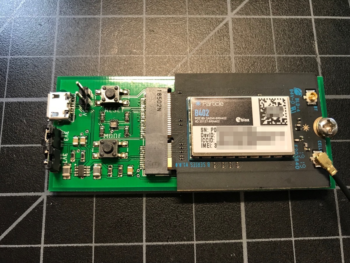
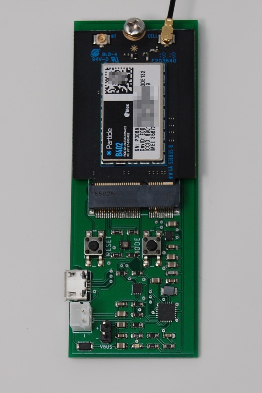
The B-Series SoM cannot be used without a base board. Typically you will create your own board, however there are two off-the-shelf options available:
B-Series Eval board
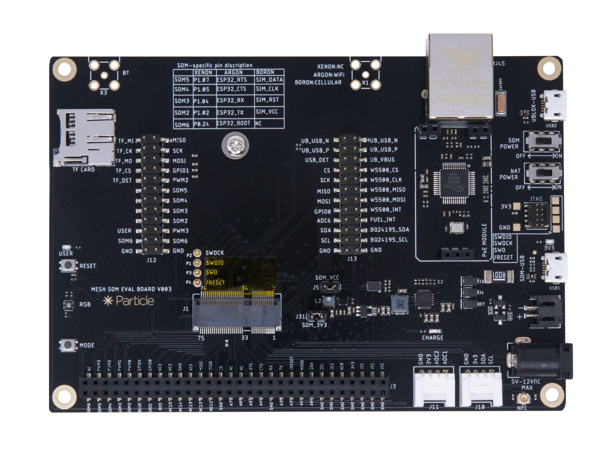
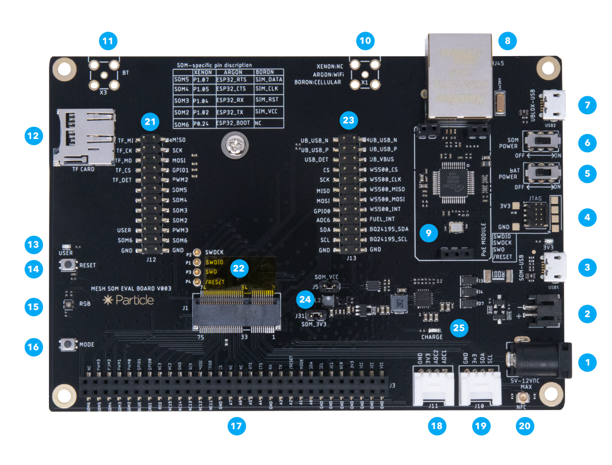
The B-Series evaluation board provides a variety of interfaces and access to all ports and pins on the B-Series SoM. You can use the expansion connector to connect the evaluation board to a breadboard for prototyping. You can also add sensors and accessories using the Grove expansion connectors.
| Num | ID | Description |
|---|---|---|
| 1 | External Power | 5-12 VDC. Minimum power requirements are 5VDC @500mA (when using the LiPo battery) or 5VDC @2000mA (without LiPo battery). |
| 2 | LiPo Battery connector | Plug in the LiPo battery here. |
| 3 | SoM USB port | This is the module's main USB port that connects to the microcontroller. |
| 4 | JTAG connector | This can plug directly into the Particle debugger ribbon cable. |
| 5 | Battery switch | Controls power between the LiPo connector and the charge controller. |
| 6 | SoM power switch | Controls 3V3 power to the SoM |
| 7 | u-blox USB port | This USB port connects directly to the u-blox module for firmware updates. |
| 8 | Ethernet connector | RJ45 connector for twisted pair Ethernet, 10 or 100 Mbit/sec. |
| 9 | PoE connector | Connect for the Particle PoE adapter for power-over-Ethernet. |
| 10 | Cellular antenna | Connector for an external SMA connected cellular antenna. |
| 11 | Bluetooth antenna | Connector for an external SMA connected antenna for Bluetooth networking. |
| 12 | TF/SD Card | MicroSD card slot. |
| 13 | User LED | Blue LED connected to pin D7. |
| 14 | Reset Button | This is same as the RESET button on the Boron. |
| 15 | RGB LED | System status indicator RGB LED. |
| 16 | Mode Button | This is the same as the MODE button on the Boron. |
| 17 | Expansion Connector | Allows easy access to SoM IO pins. |
| 18 | Grove Analog Port | Connects to Seeed Studio Grove analog and digital boards. |
| 19 | Grove I2C Port | Connects to Seeed Studio Grove I2C boards. |
| 20 | NFC Antenna | U.FL connector for an NFC antenna (optional). |
| 21 | Jumpers J12 | Enable or disable various features on the evaluation board. |
| 22 | SoM connector | M.2 connector for the B-Series SoM. |
| 23 | Jumpers J13 | Enable or disable various features on the evaluation board. |
| 24 | Power Jumpers | Enable or disable power from the evaluation board. |
| 25 | Charge LED | Indicate LiPo is charging. |
Mikroe Gen 3 SoM shield
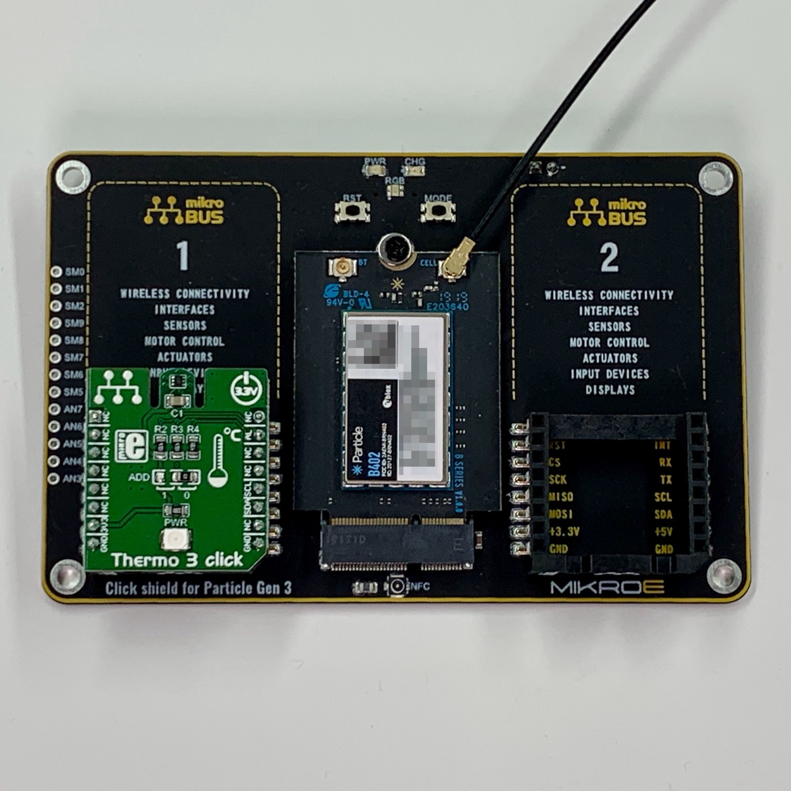
The Gen 3 SoM shield connects a B-Series SoM to mikroBUS Click boards:
| M.2 Pin | Generic SoM | Gen 3 | mikroBUS #1 | mikroBUS #2 |
|---|---|---|---|---|
| 20 | SCL | D1 | SCL | SCL |
| 22 | SDA | D0 | SDA | SDA |
| 23 | ADC0 | A0 | RST2 | |
| 33 | ADC1 | A1 | AN1 | |
| 35 | ADC2 | A2 | AN2 | |
| 36 | TX | TX/D9 | TX | TX |
| 37 | ADC3 | A3 | ||
| 38 | RX | TX/D10 | RX | RX |
| 41 | ADC4 | A4 | ||
| 43 | ADC5 | A5 | ||
| 45 | ADC6 | A6 | ||
| 47 | ADC7 | A7 | ||
| 48 | CS | D8 | CS1 | |
| 50 | MISO | MISO/D11 | MISO | MISO |
| 52 | MOSI | MOSI/D12 | MOSI | MOSI |
| 54 | SCK | SCK/D13 | SCK | SCK |
| 62 | GPIO0 | D22 | INT1 | |
| 64 | GPIO1 | D23 | INT2 | |
| 66 | PWM0 | D4 | CS2 | |
| 68 | PWM1 | D5 | PWM1 | |
| 70 | PWM2 | D6 | PWM2 | |
| 72 | PWM3 | D7 | RST1 |
There is a huge library of mikroBUS Click expansion boards, however the caveat is that most of them do not already have a Particle software library. If the board is for a common sensor or chip, however, existing Particle libraries for the chip will typically work, even if not designed work with the Click.
For more information, see the Mikroe community page.
Creating a board
First SoM board tutorial
The SoM first board tutorial shows how to get started with the M.2 SoM boards by making the simplest possible design. It's an introduction to working with surface mount components you will need in order to make your own SoM base board.
Basic SoM design
This design is a bit more complicated, and includes the PMIC and Fuel Gauge chips that are present on the E-Series:
- RGB LED
- bq24195 PMIC
- MAX17043 Fuel Gauge
- USB Connector
- LiPo Connector (JST-PH)
- M.2 SoM Connector
This is the basic set of features you'll probably want to include in a LiPo battery-powered design. The Evaluation Board is also a good reference to use. This design, however, is simple enough that it can be hand-assembled, though you still need a reflow oven and some of the parts (in particular the fuel gauge and PMIC) are tiny and there are a lot of them.
This board a two-layer circuit board so it can be manufactured inexpensively and edited using the free version of Eagle CAD.
As this board doesn't really do much, you'll unlikely use it as-is, but you can use it as a tutorial for how to hook up the PMIC and fuel gauge.
Software differences
User firmware binary size
One major advantage of Gen 3 devices is that user firmware binaries in Device OS 3.1.0 and later can be up to 256 Kbytes, instead of 128 Kbytes in earlier version of Device OS and on Gen 2 devices. The larger firmware binary support will not be added to Gen 2 in the future, and will only be available on Gen 3 devices.
Flash file system
There is a flash file system (2 MB except on the Tracker which is 4 MB) for storing user data, on Gen 3 devices only.
Combined and resumable OTA
On Gen 3 devices, over-the-air (OTA) updates have two features that can improve the speed and reliability of OTA updates:
- Combined OTA can combine Device OS and user firmware updates into a single binary that requires only one download and one reboot to install.
- Resumable OTA allows an update to resume from the point it stopped, instead of starting over from the beginning if interrupted.
Asset OTA
Asset OTA (available in Device OS 5.5.0 and later), makes it possible to include bundled assets in an OTA software update that can be delivered to other processors and components in your product.
Increased API field limits
The maximum size of a variable, function parameter, or publish is 1024 bytes on the B-Series SoM vs. 864 bytes on the E-Series.
| API Field | E-Series | B-Series SoM |
|---|---|---|
| Variable Key | 64 | 64 |
| Variable Data | 864 | 1024 |
| Function Key | 64 | 64 |
| Function Argument | 864 | 1024 |
| Publish/Subscribe Event Name | 64 | 64 |
| Publish/Subscribe Event Data | 864 | 1024 |
Hardware differences
MCU
| Measure | E-Series | B-Series SoM |
|---|---|---|
| MCU | STM32F205 | nRF52840 |
| Manufacturer | ST Microelectronics | Nordic Semiconductor |
| Processor | ARM Cortex M3 | ARM Cortex M4F |
| Speed | 120 MHz | 64 MHz |
| RAM | 128 KB | 256 KB |
| Flash (MCU) | 1 MB | 1 MB |
| Flash (external) | 4 MB | |
| Hardware floating point | ✓ |
- Not all RAM is available to user applications. The Device OS firmware uses a portion of it.
BLE (Bluetooth LE)
- Bluetooth LE (BLE 5.0) is supported on B-Series SoM but not the E-Series.
NFC tag
- NFC tag mode is supported on the B-Series SoM but not the E-Series.
GPIO
There are fewer available GPIO pins on the B-Series SoM than the E-Series. If you need a large number of GPIO pins, an external GPIO expander connected by I2C or SPI is a good option.
| E-Series Pin | E-Series Pin Name | E-Series GPIO | B-Series SoM Pin | B-Series SoM Pin Name | B-Series SoM GPIO |
|---|---|---|---|---|---|
| 26 | A0 | ✓ | 23 | A0 / D19 | ✓ |
| 25 | A1 | ✓ | 33 | A1 / D18 | ✓ |
| 24 | A2 | ✓ | 35 | A2 / D17 | ✓ |
| 23 | A3 | ✓ | 37 | A3 / D16 | ✓ |
| 22 | A4 | ✓ | 41 | A4 / D15 | ✓ |
| 21 | A5 | ✓ | 43 | A5 / D14 | ✓ |
| 33 | B0 | ✓ | |||
| 32 | B1 | ✓ | |||
| 31 | B2 | ✓ | |||
| 30 | B3 | ✓ | |||
| 29 | B4 | ✓ | |||
| 28 | B5 | ✓ | |||
| 49 | C0 | ✓ | |||
| 48 | C1 | ✓ | |||
| 47 | C2 | ✓ | |||
| 46 | C3 | ✓ | |||
| 45 | C4 | ✓ | |||
| 44 | C5 | ✓ | |||
| 42 | D0 | ✓ | 22 | D0 | ✓ |
| 41 | D1 | ✓ | 20 | D1 | ✓ |
| 40 | D2 | ✓ | 42 | D2 | ✓ |
| 62 | D22 | ✓ | |||
| 64 | D23 | ✓ | |||
| 39 | D3 | ✓ | 40 | D3 | ✓ |
| 38 | D4 | ✓ | 66 | D4 | ✓ |
| 37 | D5 | ✓ | 68 | D5 | ✓ |
| 36 | D6 | ✓ | 70 | D6 | ✓ |
| 35 | D7 | ✓ | 72 | D7 | ✓ |
| 48 | D8 | ✓ | |||
| 20 | DAC / A6 | ✓ | 45 | A6 | ✓ |
| 50 | MISO / D11 | ✓ | |||
| 52 | MOSI / D12 | ✓ | |||
| 17 | RX | ✓ | 38 | RX / D10 | ✓ |
| 54 | SCK / D13 | ✓ | |||
| 16 | TX | ✓ | 36 | TX / D9 | ✓ |
| 19 | WKP / A7 | ✓ | 47 | A7 | ✓ |
The MCP23008 is an 8-port GPIO expander that connects to I2C and works well with Gen 3 devices. You can connect up to 8 of them to a single I2C interface. the MCP23017 has 16-ports, and you can also connect 8 of them, for a total of 128 GPIO ports.
The application note AN013 Tracker GPIO shows how you can add additional GPIO to your Tracker One using the external M8 connector, however the same technique can also be used with the B-Series SoM. It includes both 3.3V and 5V design options.
5V tolerance
The other difference in the GPIO between Gen 2 and Gen 3 is with 5V tolerance. While both devices are 3.3V devices and only will drive 3.3V, the I/O pins on Gen 2 devices (with the exception of A3 and A6) are 5V tolerant. This allows a Gen 2 device to connect to some 5V peripherals directly.
You must not connect 5V peripherals to a Gen 3 device. This includes GPIO, ports (serial, I2C, SPI), and ADC.
Interfacing with 5V peripherals can be done with a level shifter, a MOSFET, or a 5V GPIO expander.
Beware of leakage current
If you have circuitry that can disconnect the nRF52840 MCU 3V3 power, beware of situations where current can leak into GPIO pins from an external supply.
For example, if you have 3V3 disconnect circuitry but have pull-ups to non-disconnected power, when MCU 3V3 is powered down current can flow into the GPIO causing the MCU to not fully power down. This can prevent the MCU from resetting when power is reapplied. It will also cause excess power consumption when powered down.
SPI
- The B-Series SoM and E-Series both have two SPI ports.
- In most cases, you can share a single SPI bus with many peripherals.
- On the E-Series, SPI1 and SPI2 share the same MCU SPI interface but have different pin locations. You can only use one or the other.
| E-Series Pin | E-Series Pin Name | E-Series SPI | B-Series SoM Pin | B-Series SoM Pin Name | B-Series SoM SPI |
|---|---|---|---|---|---|
| 24 | A2 | SPI (SS) | 35 | A2 / D17 | |
| 23 | A3 | SPI (SCK) | 37 | A3 / D16 | |
| 22 | A4 | SPI (MISO) | 41 | A4 / D15 | |
| 21 | A5 | SPI (MOSI) | 43 | A5 / D14 | |
| 48 | C1 | SPI2 (MOSI) | |||
| 47 | C2 | SPI2 (MISO) | |||
| 46 | C3 | SPI2 (SCK) | |||
| 40 | D2 | SPI1 (MOSI) | 42 | D2 | SPI1 (SCK) |
| 39 | D3 | SPI1 (MISO) | 40 | D3 | SPI1 (MOSI) |
| 38 | D4 | SPI1 (SCK) | 66 | D4 | SPI1 (MISO) |
| 37 | D5 | SPI1 (SS) | 68 | D5 | |
| 48 | D8 | SPI (SS) | |||
| 50 | MISO / D11 | SPI (MISO) | |||
| 52 | MOSI / D12 | SPI (MOSI) | |||
| 54 | SCK / D13 | SPI (SCK) |
Serial (UART)
There are more UART ports on the Gen 2 devices than Gen 3. If you need more hardware serial ports, the best option is to use the SC16IS740 or its relatives like the SC16IS750. These devices connect by I2C or SPI, and you can add multiple ports this way.
Serial baud rates
| Baud Rate | Gen 2 | Gen 3 |
|---|---|---|
| 1200 | ✓ | ✓ |
| 2400 | ✓ | ✓ |
| 4800 | ✓ | ✓ |
| 9600 | ✓ | ✓ |
| 19200 | ✓ | ✓ |
| 28800 | ✓ | |
| 38400 | ✓ | ✓ |
| 57600 | ✓ | ✓ |
| 76800 | ✓ | |
| 115200 | ✓ | ✓ |
| 230400 | ✓ | ✓ |
| 250000 | ✓ | |
| 460800 | ✓ | |
| 921600 | ✓ | |
| 1000000 | ✓ |
Serial configurations
| Constant | Description | Gen 2 | Gen 3 |
|---|---|---|---|
| SERIAL_8N1 | 8 data bits, no parity, 1 stop bit (default) | ✓ | ✓ |
| SERIAL_8N2 | 8 data bits, no parity, 2 stop bits | ✓ | |
| SERIAL_8E1 | 8 data bits, even parity, 1 stop bit | ✓ | ✓ |
| SERIAL_8E2 | 8 data bits, even parity, 2 stop bits | ✓ | |
| SERIAL_8O1 | 8 data bits, odd parity, 1 stop bit | ✓ | |
| SERIAL_8O2 | 8 data bits, odd parity, 2 stop bits | ✓ | |
| SERIAL_9N1 | 9 data bits, no parity, 1 stop bit | ✓ | |
| SERIAL_9N2 | 9 data bits, no parity, 2 stop bits | ✓ | |
| SERIAL_7O1 | 7 data bits, odd parity, 1 stop bit | ✓ | |
| SERIAL_7O2 | 7 data bits, odd parity, 1 stop bit | ✓ | |
| SERIAL_7E1 | 7 data bits, even parity, 1 stop bit | ✓ | |
| SERIAL_7E2 | 7 data bits, even parity, 1 stop bit | ✓ | |
| LIN_MASTER_13B | 8 data bits, no parity, 1 stop bit, LIN Master mode with 13-bit break generation | ✓ | |
| LIN_SLAVE_10B | 8 data bits, no parity, 1 stop bit, LIN Slave mode with 10-bit break detection | ✓ | |
| LIN_SLAVE_11B | 8 data bits, no parity, 1 stop bit, LIN Slave mode with 11-bit break detection | ✓ |
- Using an I2C or SPI UART like the SC16IS750 is also a good way to add support for other bit length, parity, and stop bit options on Gen 3 devices.
| E-Series Pin | E-Series Pin Name | E-Series Serial | B-Series SoM Pin | B-Series SoM Pin Name | B-Series SoM Serial |
|---|---|---|---|---|---|
| 49 | C0 | Serial5_RX | |||
| 48 | C1 | Serial5_TX | |||
| 47 | C2 | Serial4 RX | |||
| 46 | C3 | Serial4 TX | |||
| 40 | D2 | 42 | D2 | Serial1 RTS | |
| 39 | D3 | 40 | D3 | Serial1 CTS | |
| 52 | RGBB | Serial2 (RX) | 65 | RGBB | |
| 53 | RGBG | Serial2 (TX) | 63 | RGBG | |
| 17 | RX | Serial1 (RX) | 38 | RX / D10 | Serial1 RX |
| 16 | TX | Serial1 (TX) | 36 | TX / D9 | Serial1 TX |
Analog input (ADC)
The B-Series SoM does not have an many ADC ports as the E-Series. You can add additional ADC ports using a SPI or I2C ADC.
| E-Series Pin | E-Series Pin Name | E-Series ADC | B-Series SoM Pin | B-Series SoM Pin Name | B-Series SoM ADC |
|---|---|---|---|---|---|
| 26 | A0 | ✓ | 23 | A0 / D19 | ✓ |
| 25 | A1 | ✓ | 33 | A1 / D18 | ✓ |
| 24 | A2 | ✓ | 35 | A2 / D17 | ✓ |
| 23 | A3 | ✓ | 37 | A3 / D16 | ✓ |
| 22 | A4 | ✓ | 41 | A4 / D15 | ✓ |
| 21 | A5 | ✓ | 43 | A5 / D14 | ✓ |
| 31 | B2 | ✓ | |||
| 30 | B3 | ✓ | |||
| 29 | B4 | ✓ | |||
| 28 | B5 | ✓ | |||
| 20 | DAC / A6 | ✓ | 45 | A6 | ✓ |
| 19 | WKP / A7 | ✓ | 47 | A7 | ✓ |
PWM (Pulse-width modulation)
These are differences in pins that support PWM between the E-Series and B-Series SoM.
| E-Series Pin | E-Series Pin Name | E-Series PWM | B-Series SoM Pin | B-Series SoM Pin Name | B-Series SoM PWM | B-Series SoM Hardware Timer |
|---|---|---|---|---|---|---|
| 26 | A0 | 23 | A0 / D19 | ✓ | PWM2 | |
| 25 | A1 | 33 | A1 / D18 | ✓ | PWM2 | |
| 22 | A4 | ✓ | 41 | A4 / D15 | ||
| 21 | A5 | ✓ | 43 | A5 / D14 | ||
| 33 | B0 | ✓ | ||||
| 32 | B1 | ✓ | ||||
| 31 | B2 | ✓ | ||||
| 30 | B3 | ✓ | ||||
| 45 | C4 | ✓ | ||||
| 44 | C5 | ✓ | ||||
| 42 | D0 | ✓ | 22 | D0 | ||
| 41 | D1 | ✓ | 20 | D1 | ||
| 40 | D2 | ✓ | 42 | D2 | ||
| 39 | D3 | ✓ | 40 | D3 | ||
| 38 | D4 | 66 | D4 | ✓ | PWM1 | |
| 37 | D5 | 68 | D5 | ✓ | PWM1 | |
| 36 | D6 | 70 | D6 | ✓ | PWM1 | |
| 35 | D7 | 72 | D7 | ✓ | PWM0 | |
| 20 | DAC / A6 | 45 | A6 | ✓ | PWM2 | |
| 17 | RX | ✓ | 38 | RX / D10 | ||
| 16 | TX | ✓ | 36 | TX / D9 | ||
| 19 | WKP / A7 | ✓ | 47 | A7 | ✓ | PWM2 |
PWM - Gen 3
On Gen 3 devices, the PWM frequency is from 5 Hz to analogWriteMaxFrequency(pin) (default is 500 Hz).
On the B-Series SoM, pins D4, D5, D7, A0, A1, A6, and A7 can be used for PWM. Pins are assigned a PWM group. Each group must share the same frequency and resolution, but individual pins in the group can have a different duty cycle.
- Group 2: Pins A0, A1, A6, and A7.
- Group 1: Pins D4, D5, and D6.
- Group 0: Pin D7 and the RGB LED. This must use the default resolution of 8 bits (0-255) and frequency of 500 Hz.
It is also possible to add an external PWM driver such as the PCA9685 which adds 16 outputs via I2C. You can add 62 of these to a single I2C bus for 992 PWM outputs! The Adafruit_PWMServoDriver library supports this chip on all Particle devices.
PWM - Gen 2
On the Electron and E-Series, this function works on pins D0, D1, D2, D3, A4, A5, WKP, RX, TX, B0, B1, B2, B3, C4, and C5 with a caveat: PWM timer peripheral is duplicated on two pins (A5/D2) and (A4/D3) for 7 total independent PWM outputs. For example: PWM may be used on A5 while D2 is used as a GPIO, or D2 as a PWM while A5 is used as an analog input. However A5 and D2 cannot be used as independently controlled PWM outputs at the same time.
Internal pull-up or pull-down
Internal (MCU) pull-up and pull-down can be enabled using the pinMode() function and INPUT_PULLUP or INPUT_PULLDOWN.
On both the B-Series SoM (Gen 3), the internal pull is approximately 16K. On the E-Series it is approximately 40K.
Retained memory
Retained memory, also referred to as Backup RAM or SRAM, that is preserved across device reset.
On both the Boron and B-Series SoM, retained memory is 3068 bytes, same as the E-Series.
The flash file system on Gen 3 devices can also be used for data storage, however care must be taken to avoid excessive wear of the flash for frequently changing data.
Interrupts
Interrupts - Gen 2
Not supported on the Electron/E series (you can't use attachInterrupt on these pins):
- D0, A5 (shared with MODE button)
- D7 (shared with BATT_INT_PC13)
- C1 (shared with RXD_UC)
- C2 (shared with RI_UC)
No restrictions on the Electron/E-Series (all of these can be used at the same time):
- D5, D6
Shared on the Electron/E-Series (only one pin for each bullet item can be used at the same time):
- D1, A4, B1
- D2, A0, A3
- D3, DAC
- D4, A1
- A2, C0
- A7 (WKP), B2, B4
- B0, C5
- B3, B5
- C3, TX
- C4, RX
Interrupts - Gen 3
There is a limit of 8 pins with interrupt handlers, however the selection of pins is not restricted.
DAC
Gen 2 devices have two DAC (digital-to-analog converter), on pins A3 and A6.
Gen 3 devices do not have built-in DAC, however they can easily be added by I2C or SPI to your base board.
CAN bus
- Gen 3 devices do not support CAN on the MCU.
- The Tracker SoM includes CAN via a MCP25625 CAN interface with integrated transceiver.
- Both the MCP2515 and MCP25625 work with the library used on the Tracker and can be used to add CAN to other Gen 3 devices.
I2S (Sound)
- The E-Series theoretically had I2S sound available on pins D1 and D2, however there has never been support for it in Device OS.
- I2S is available on Gen 3 devices including the B-Series SoM on any GPIO pins using a 3rd-party library.
Sleep modes
- In general, Gen 3 devices use less power in all modes.
- In
HIBERNATEmode, the RTC (real time clock) does not run on Gen 3 devices, so you cannot wake by time fromHIBERNATEmode (formerly known asSLEEP_MODE_DEEP). - However, you can wake by time from
ULTRA_LOW_POWERmode, and it uses less power than the Gen 2HIBERNATEmode. - On Gen 2 devices, you can only wake from
HIBERNATEwith a rising signal onWKP(A7). Gen 3 devices can wake fromHIBERNATEon any pin, rising or falling. - On Gen 2 (STM32F205) devices, if you try to go into
HIBERNATEmode with WKP already high, the device will go into sleep and will not wake up by time or pin change, essentially rendering it unable to wake until reset manually. This problem does not occur on Gen 3 devices.
RTC (Real-time clock)
- The E-Series module has the ability to use an external lithium coin cell or supercap to power the RTC when the MCU is unpowered. This feature is difficult to access on the Electron (requires removing a resistor on the module) and does not exist on Gen 3 devices.
- The RTC on Gen 3 devices is not really a real-time clock. It's basically just a counter, and some advanced wakeup features are not possible on Gen 3 devices. These features were not enabled by Device OS on Gen 2 devices, either, so this is generally not an issue.
- On Gen 3 devices, in
HIBERNATEsleep mode the RTC does not run, so it is not possible to wake by time, and the system clock will not be set until you connect to the cloud again.ULTRA_LOW_POWERis recommended instead. - The Tracker SoM has a separate real-time clock and watchdog (AM1805) chip allowing it to wake from
HIBERNATEbased on time.
SWD/JTAG
- Gen 2 devices support SWD on D6 and D7, and full JTAG on D3, D4, D5, D6, and D7.
- Gen 3 devices only support SWD, and do so via a dedicated debug connector.
- The Boron has the debug connector on top of the module.
- The B-Series SoM has SWD on pads on the bottom of the SoM. The evaluation board connects to these with pogo pins and breaks out to the same 2x5 connector that is on the Boron.
JTAG pin warning - Gen 2
On Gen 2 devices, beware when using pins D3, D5, D6, and D7 as OUTPUT controlling external devices. After reset, these pins will be briefly taken over for JTAG/SWD, before being restored to the default high-impedance INPUT state during boot.
- D3, D5, and D7 are pulled high with a pull-up
- D6 is pulled low with a pull-down
- D4 is left floating
The brief change in state (especially when connected to a MOSFET that can be triggered by the pull-up or pull-down) may cause issues when using these pins in certain circuits. Using STARTUP will not prevent this!
This is not an issue with Gen 3 devices that have dedicated SWD pins.
If you are relying on this behavior for external circuits, you should instead use a hardware pull-up or pull-down on Gen 3 devices. The pins default to high-impedance state, and this means they will stay in this state when in the bootloader, DFU mode, and safe mode.
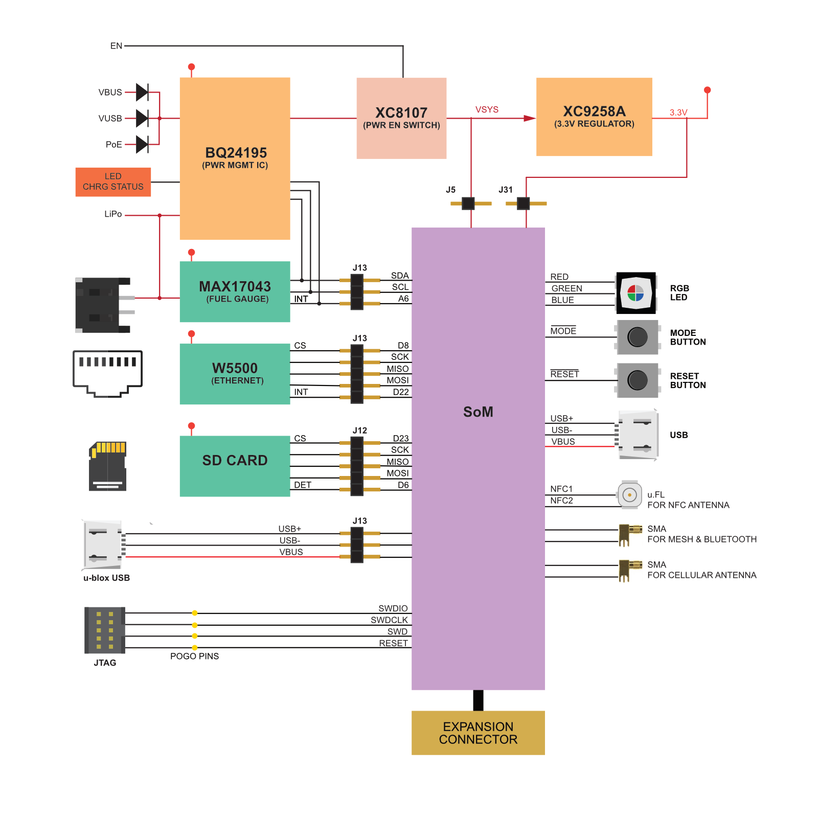
PMIC and Fuel gauge
The E-Series, E-Series, Boron, and Tracker SoM all include the PMIC (bq24195) and battery fuel gauge (MAX17043) on the module itself.
On the B-Series SoM, the PMIC and fuel gauge are optional. For example, if you are powering by an external power supply and not using a battery, you can omit the components entirely.
USB
- Both the E-Series and B-Series SoM assume the USB connector will be mounted on your base board. It is recommended that you add one to your base board for programming and troubleshooting.
- Gen 2 devices can emulate a USB mouse or keyboard over the USB port. This feature is not available on Gen 3.
- Gen 2 devices can support two separate USB serial emulation streams over the USB port. Gen 3 devices only support the normal
Serialinterface.
| USB Feature | E-Series | B-Series SoM |
|---|---|---|
Secondary USB serial emulation USBSerial1 |
✓ | |
| USB keyboard emulation | ✓ | |
| USB mouse emulation | ✓ |
NFC tag
The B-Series SoM has NFC Tag support, however you must add a U.FL antenna connector to your base board to use it.
Note that this only supports emulating an NFC tag that can be read by an another reader or smartphone. It does not allow the B-Series SoM to detect other tags!
PMIC Notes
When using the B-Series SoM with a bq24195 PMIC, note the following:
By default, the bq24195 sets the input current limit, which affects powering by VIN and VUSB, to 100 mA. This affects the VSYS output of the PMIC, which powers both the cellular modem and 3V3 supply, and is not enough to power the B-Series SoM in normal operation.
If your device has the default firmware (Tinker), it will attempt to connect to the cloud, brown out due to insufficient current, then the device will reset. This may result in what appears to be the status LED blinking white, but is actually rolling reboot caused by brownout.
A factory new B-Series SoM does not enable the PMIC setup. To enable the use of the bq21415, you must enable the system power feature PMIC_DETECTION in your code. This defaults to off because the B-Series SoM can be used without a PMIC, or with a different PMIC, and also requires I2C on D0/D1, and some base boards may use those pins as GPIO.
Because the input current limit does not affect the battery input (Li+), for troubleshooting purposes it can be helpful to attach a battery to help rule out input current limit issues. It's also possible to supply 3.7V via a bench power supply to the battery input, instead of VIN.
The input current limit can result in a situation where you can't bring up a B-Series SoM because it browns out continuously, but also cannot flash code to it to stop if from browning out. There are two general solutions:
- Attach a battery or supply by Li+ when bringing up a board.
- Use SWD/JTAG and reset halt the MCU. This will prevent it from connecting to the cloud, so you can flash Device OS and firmware to it by SWD.
The input current limit is actually controlled by three factors:
- The power source max current setting in the PMIC. The default is 900 mA. It can be set to 100, 150, 500, 900, 1200, 1500, 2000, or 3000 mA.
- It is also limited by the hardware ILIM resistor. On Particle devices with a built-in PMIC, this is set to 1590 mA, but if you are implementing your own PMIC hardware, you can adjust this higher.
- When connected by USB, it will use DPDM, current negotiation via the USB DP (D+) and DM (D-) lines.
Note that some 2A tablet chargers and multi-port USB power supplies supply 2A but do not implement DPDM; these will be treated as if VIN was used, and you must set the power source current, otherwise the input current will be limited to 900 mA, which is not enough to power a 2G/3G cellular modem without an attached battery.
Antennas
The B-Series SoM has U.FL antenna connectors for BLE and cellular antennas. A connector for NFC can be added from your base board.
The E-Series has a U.FL connector for the cellular antenna, and does not have BLE or NFC tag capabilities.
Both require an external cellular antenna.
| Device | SKU | Included | Antenna | Alternate | Lifecycle |
|---|---|---|---|---|---|
| B-Series LTE CAT-1/3G (NorAm, EtherSIM), [x1] | B504MEA | ✓ | PARANTCW1EA | Deprecated | |
| B-Series LTE CAT-1/3G (NorAm, EtherSIM), [x50] | B504MTY | PARANTCW1TY | Deprecated | ||
| B-Series LTE CAT-1/3G (NorAm, EtherSIM+), [x1] | B504EMEA | ✓ | PARANTCW1EA | GA | |
| B-Series LTE CAT-1/3G (NorAm, EtherSIM+), [x50] | B504EMTY | PARANTCW1TY | GA | ||
| B-Series LTE CAT-1/3G/2G (Europe, EtherSIM) [x1] | B524MEA | ✓ | ANTCW2EA | GA | |
| B-Series LTE CAT-1/3G/2G (Europe, EtherSIM), Tray [x50] | B524MTY | ANTCW2TY | GA | ||
| B-Series LTE CAT-1/3G/2G (Europe) [x1] | B523MEA | ✓ | ANTCW2EA | Deprecated | |
| B-Series LTE CAT-1/3G/2G (Europe), Tray [x50] | B523MTY | ANTCW2TY | NRND | ||
| B-Series LTE CAT-M1 (NorAm), [x1] | B402MEA | ✓ | ANTCW2EA | Deprecated | |
| B-Series LTE CAT-M1 (NorAm), Tray [x50] | B402MTY | ANTCW2TY | Deprecated | ||
| B-Series LTE-M (NorAm, EtherSIM), [x1] | B404MEA | ✓ | ANTCW2EA | Deprecated | |
| B-Series LTE-M (NorAm, EtherSIM), [x1] | B404XMEA | ✓ | PARANTC41EA | ANT-FLXU3 | GA |
| B-Series LTE-M (NorAm, EtherSIM), Tray [x50] | B404MTY | ANTCW2TY | NRND | ||
| B-Series LTE-M (NorAm, EtherSIM), Tray [x50] | B404XMTY | PARANTC41TY | ANT-FLXU-503 | GA | |
| E-Series 2G/3G (Global - E310) Evaluation Kit, [x1] | E310KIT | ✓ | ANTELEC | ANTCW2EA2 | NRND |
| E-Series 2G/3G (Global - E310), [x1] | E310MOD1 | ✓ | ANTELEC | ANTCW2EA2 | Deprecated |
| E-Series 2G/3G (Global - E310), Tray [x50] | E310TRAY50 | ANTELEC50 | ANTCW2TY2 | Deprecated | |
| E-Series 2G/3G (Global - E313), [x1] | E313EA | ✓ | ANTELEC | ANTCW2EA2 | Deprecated |
| E-Series 2G/3G (Global - E313), Tray [x50] | E313TRAY50 | ANTELEC50 | ANTCW2TY2 | End of life | |
| E-Series 2G/3G (Global - E314) Evaluation Kit, [x1] | E314KIT | ✓ | ANTELEC | ANTCW2EA2 | NRND |
| E-Series 2G/3G (Global - E314), [x1] | E314MOD1 | ✓ | ANTELEC | ANTCW2EA2 | Deprecated |
| E-Series 2G/3G (Global - E314), Tray [x50] | E314TRAY50 | ANTELEC50 | ANTCW2TY2 | NRND | |
| E-Series LTE CAT-M1 (NorAm, EtherSIM), Tray [x50] | E404TRAY50 | ANT-FLXU-50 | ANTCW2TY2 | Deprecated | |
| E-Series LTE CAT-M1 (NorAm, EtherSIM), Tray [x50] | E404XTRAY50 | ANT-FLXU-50 | PARANTC41TY2 | GA | |
| E-Series LTE CAT-M1 (NorAm) Evaluation Kit, [x1] | E402KIT | ✓ | ANT-FLXU | ANTCW2EA2 | NRND |
| E-Series LTE CAT-M1 (NorAm), [x1] | E402MOD1 | ✓ | ANT-FLXU | ANTCW2EA2 | Deprecated |
| E-Series LTE CAT-M1 (NorAm), Tray [x50] | E402TRAY50 | ✓ | ANT-FLXU-50 | ANTCW2TY2 | NRND |
| E-Series LTE-M (NorAm, EtherSIM) Evaluation Kit, [x1] | E404KIT | ✓ | ANT-FLXU | ANTCW2EA2 | NRND |
| E-Series LTE-M (NorAm, EtherSIM), [x1] | E404MOD1 | ✓ | ANT-FLXU | ANTCW2EA2 | NRND |
2This device originally shipped with one antenna (ANTELEC or ANT-FLXU) however the ANTCW2EA is listed as an alternative. The ANTCW2EA (or ANTCW2TY) is recommended as most new designs will use this antenna and using this antenna will reduce the number of SKUs you need to stock when building a product at tray quantities.
| Dimension | PARANTCW1EA | PARANTC41EA | ANTCW2EA | ANT-FLXU | ANTELEC |
|---|---|---|---|---|---|
| Tray SKU | PARANTCW1TY | PARANTC41TY | ANTCW2TY | ANT-FLXU-50 | ANTELEC50 |
| Length | 116mm | 122.1mm | 97.0mm | 96.0mm | 80.0mm |
| Width | 27mm | 12.8mm | 21.0mm | 21.0mm | 20.0mm |
| Thickness | 0.2mm | 0.2mm | 0.2mm | 0.2mm | 0.2mm |
| Cable Length | 189.5mm | 183mm | 160mm | 150mm | 164mm |
PARANTC41EA/PARANTC41TY are slightly longer than ANTCW2EA/ANTCW2TY. The antenna can be bent when being placed inside an enclosure. There are a couple restrictions to ensure good performance:
- Do not bend more the 90 degrees. Right angle turns are acceptable, but do not fold the antenna over on itself.
- The antenna should not be creased when it is bent into position. A crease can damage the internal structure of the antenna.
- The antenna should always be affixed along its entire length. Do not affix a portion of the antenna and leave a portion free floating.
- All portions of the antenna should maintain proper spacing from electronics, grounded metal, or active metal.
- Recommended: 12mm
- Minimum: 8mm
- Ideally when placing the antenna it should not have a bend in it, but following the above guidelines, there should be minimal performance degradation.
Full module pin comparison
3V3
| E-Series | B-Series SoM | ||
|---|---|---|---|
| ∆ | Pin Number | 9 | 10 |
| Pin Name | 3V3 | 3V3 | |
| ∆ | Description | Regulated 3.3V DC output, maximum load 800 mA. Cannot be used as a power input. | System power in, supply a fixed 3.0-3.6v power. |
A0
| E-Series | B-Series SoM | ||
|---|---|---|---|
| ∆ | Pin Number | 26 | 23 |
| Pin Name | A0 | A0 | |
| ∆ | Pin Alternate Name | n/a | D19 |
| ∆ | Description | A0 Analog in, GPIO | A0 Analog in, GPIO, PWM |
| Supports digitalRead | Yes | Yes | |
| Supports digitalWrite | Yes | Yes | |
| Supports analogRead | Yes | Yes | |
| ∆ | Supports analogWrite (PWM) | No | Yes |
| ∆ | Supports tone | No | A0, A1, A6, and A7 must have the same frequency. |
| ∆ | Supports attachInterrupt | Yes. D2, A0, and A3 share the same interrupt handler. | Yes. You can only have 8 active interrupt pins. |
| ∆ | Internal pull resistance | 40K | 13K |
| ∆ | Input is 5V Tolerant | Yes | No |
A1
| E-Series | B-Series SoM | ||
|---|---|---|---|
| ∆ | Pin Number | 25 | 33 |
| Pin Name | A1 | A1 | |
| ∆ | Pin Alternate Name | n/a | D18 |
| ∆ | Description | A1 Analog in, GPIO | A1 Analog in, GPIO, PWM |
| Supports digitalRead | Yes | Yes | |
| Supports digitalWrite | Yes | Yes | |
| Supports analogRead | Yes | Yes | |
| ∆ | Supports analogWrite (PWM) | No | Yes |
| ∆ | Supports tone | No | A0, A1, A6, and A7 must have the same frequency. |
| ∆ | Supports attachInterrupt | Yes. D4 and A1 share the same interrupt handler. | Yes. You can only have 8 active interrupt pins. |
| ∆ | Internal pull resistance | 40K | 13K |
| ∆ | Input is 5V Tolerant | Yes | No |
A2
| E-Series | B-Series SoM | ||
|---|---|---|---|
| ∆ | Pin Number | 24 | 35 |
| Pin Name | A2 | A2 | |
| ∆ | Pin Alternate Name | n/a | D17 |
| ∆ | Description | A2 Analog in, GPIO, SPI SS | A2 Analog in, GPIO |
| Supports digitalRead | Yes | Yes | |
| Supports digitalWrite | Yes | Yes | |
| Supports analogRead | Yes | Yes | |
| ∆ | SPI interface | SS. Use SPI object. This is only the default SS/CS pin, you can use any GPIO instead. | n/a |
| ∆ | Supports attachInterrupt | Yes. A2 and C0 share the same interrupt handler. | Yes. You can only have 8 active interrupt pins. |
| ∆ | Internal pull resistance | 40K | 13K |
| ∆ | Input is 5V Tolerant | Yes | No |
A3
| E-Series | B-Series SoM | ||
|---|---|---|---|
| ∆ | Pin Number | 23 | 37 |
| Pin Name | A3 | A3 | |
| ∆ | Pin Alternate Name | n/a | D16 |
| ∆ | Description | A3 True analog out, analog in, GPIO. | A3 Analog in, GPIO |
| Supports digitalRead | Yes | Yes | |
| Supports digitalWrite | Yes | Yes | |
| Supports analogRead | Yes | Yes | |
| ∆ | Supports analogWrite (DAC) | Yes | No |
| ∆ | SPI interface | SCK. Use SPI object. | n/a |
| ∆ | Supports attachInterrupt | Yes. D2, A0, and A3 share the same interrupt handler. | Yes. You can only have 8 active interrupt pins. |
| ∆ | Internal pull resistance | 40K | 13K |
A4
| E-Series | B-Series SoM | ||
|---|---|---|---|
| ∆ | Pin Number | 22 | 41 |
| Pin Name | A4 | A4 | |
| ∆ | Pin Alternate Name | n/a | D15 |
| ∆ | Description | A4 Analog in, GPIO, SPI MISO. | A4 Analog in, GPIO |
| Supports digitalRead | Yes | Yes | |
| Supports digitalWrite | Yes | Yes | |
| Supports analogRead | Yes | Yes | |
| ∆ | Supports analogWrite (PWM) | Yes. D3 and A4 share the same PWM channel and the PWM duty cycle is set for both. | No |
| ∆ | Supports tone | Yes. D3 and A4 share the same PWM channel and only one frequency can be set for both. | No |
| ∆ | SPI interface | MISO. Use SPI object. | n/a |
| ∆ | Supports attachInterrupt | Yes. D1 and A4 share the same interrupt handler. | Yes. You can only have 8 active interrupt pins. |
| ∆ | Internal pull resistance | 40K | 13K |
| ∆ | Input is 5V Tolerant | Yes | No |
A5
| E-Series | B-Series SoM | ||
|---|---|---|---|
| ∆ | Pin Number | 21 | 43 |
| Pin Name | A5 | A5 | |
| ∆ | Pin Alternate Name | n/a | D14 |
| ∆ | Description | A5 Analog in, GPIO, SPI MOSI. | A5 Analog in, GPIO |
| Supports digitalRead | Yes | Yes | |
| Supports digitalWrite | Yes | Yes | |
| Supports analogRead | Yes | Yes | |
| ∆ | Supports analogWrite (PWM) | Yes. D2 and A5 share the same PWM channel and the PWM duty cycle is set for both. | No |
| ∆ | Supports tone | Yes. D2 and A5 share the same PWM channel and only one frequency can be set for both. | No |
| ∆ | SPI interface | MOSI. Use SPI object. | n/a |
| ∆ | Supports attachInterrupt | No | Yes. You can only have 8 active interrupt pins. |
| ∆ | Internal pull resistance | 40K | 13K |
| ∆ | Input is 5V Tolerant | Yes | No |
AGND
| Added to B-Series SoM | |
|---|---|
| Pin Number | 39 |
| Pin Name | AGND |
| Description | Analog Ground. |
B0
| Removed from E-Series | |
|---|---|
| Pin Number | 33 |
| Pin Name | B0 |
| Description | B0, GPIO, PWM |
| Supports digitalRead | Yes |
| Supports digitalWrite | Yes |
| Supports analogWrite (PWM) | Yes |
| Supports tone | Yes |
| Supports attachInterrupt | Yes. B0 and C5 share the same interrupt handler. |
| Internal pull resistance | 40K |
| Input is 5V Tolerant | Yes |
B1
| Removed from E-Series | |
|---|---|
| Pin Number | 32 |
| Pin Name | B1 |
| Description | B1, GPIO, PWM |
| Supports digitalRead | Yes |
| Supports digitalWrite | Yes |
| Supports analogWrite (PWM) | Yes |
| Supports tone | Yes |
| Supports attachInterrupt | Yes. D1, A4, and B1 share the same interrupt handler. |
| Internal pull resistance | 40K |
| Input is 5V Tolerant | Yes |
B2
| Removed from E-Series | |
|---|---|
| Pin Number | 31 |
| Pin Name | B2 |
| Description | B2, analog in, GPIO, PWM |
| Supports digitalRead | Yes |
| Supports digitalWrite | Yes |
| Supports analogRead | Yes |
| Supports analogWrite (PWM) | Yes |
| Supports tone | Yes |
| Supports attachInterrupt | Yes. A7 (WKP), B2, and B4 share the same interrupt handler. |
| Internal pull resistance | 40K |
| Input is 5V Tolerant | Yes |
B3
| Removed from E-Series | |
|---|---|
| Pin Number | 30 |
| Pin Name | B3 |
| Description | B3, analog in, GPIO, PWM |
| Supports digitalRead | Yes |
| Supports digitalWrite | Yes |
| Supports analogRead | Yes |
| Supports analogWrite (PWM) | Yes |
| Supports tone | Yes |
| Supports attachInterrupt | Yes. B3 and B5 share the same interrupt handler. |
| Internal pull resistance | 40K |
| Input is 5V Tolerant | Yes |
B4
| Removed from E-Series | |
|---|---|
| Pin Number | 29 |
| Pin Name | B4 |
| Description | B4 Analog in, GPIO |
| Supports digitalRead | Yes |
| Supports digitalWrite | Yes |
| Supports analogRead | Yes |
| Supports attachInterrupt | Yes. A7 (WKP), B2, and B4 share the same interrupt handler. |
| Internal pull resistance | 40K |
| Input is 5V Tolerant | Yes |
B5
| Removed from E-Series | |
|---|---|
| Pin Number | 28 |
| Pin Name | B5 |
| Description | B5 Analog in, GPIO |
| Supports digitalRead | Yes |
| Supports digitalWrite | Yes |
| Supports analogRead | Yes |
| Supports attachInterrupt | Yes. B3 and B5 share the same interrupt handler. |
| Internal pull resistance | 40K |
| Input is 5V Tolerant | Yes |
C0
| Removed from E-Series | |
|---|---|
| Pin Number | 49 |
| Pin Name | C0 |
| Description | Serial5 RX (received data), GPIO. |
| Supports digitalRead | Yes |
| Supports digitalWrite | Yes |
| UART serial | RX. Use Serial5 object. |
| Supports attachInterrupt | Yes. A2 and C0 share the same interrupt handler. |
| Internal pull resistance | 40K |
| Input is 5V Tolerant | Yes |
C1
| Removed from E-Series | |
|---|---|
| Pin Number | 48 |
| Pin Name | C1 |
| Description | Serial5 TX (trasmitted data), SPI2, GPIO. |
| Supports digitalRead | Yes |
| Supports digitalWrite | Yes |
| UART serial | TX. Use Serial5 object. |
| SPI interface | MOSI. Use SPI2 object. |
| Internal pull resistance | 40K |
| Input is 5V Tolerant | Yes |
C2
| Removed from E-Series | |
|---|---|
| Pin Number | 47 |
| Pin Name | C2 |
| Description | Serial4 RX (received data), SPI2, GPIO. |
| Supports digitalRead | Yes |
| Supports digitalWrite | Yes |
| UART serial | RX. Use Serial4 object. |
| SPI interface | MISO. Use SPI2 object. |
| Internal pull resistance | 40K |
| Input is 5V Tolerant | Yes |
C3
| Removed from E-Series | |
|---|---|
| Pin Number | 46 |
| Pin Name | C3 |
| Description | Serial4 TX (transmitted data), SPI2, GPIO. |
| Supports digitalRead | Yes |
| Supports digitalWrite | Yes |
| UART serial | TX. Use Serial4 object. |
| SPI interface | SCK. Use SPI2 object. |
| Supports attachInterrupt | Yes. C3 and TX share the same interrupt handler. |
| Internal pull resistance | 40K |
| Input is 5V Tolerant | Yes |
C4
| Removed from E-Series | |
|---|---|
| Pin Number | 45 |
| Pin Name | C4 |
| Description | I2C, CAN, GPIO. |
| Supports digitalRead | Yes |
| Supports digitalWrite | Yes |
| Supports analogWrite (PWM) | Yes |
| Supports tone | Yes |
| I2C interface | SDA. Use Wire1 object. You can only use Wire or Wire1, not both! |
| Supports attachInterrupt | Yes. C4 and RX share the same interrupt handler. |
| CAN interface | CAN1_TX |
| Internal pull resistance | 40K |
| Input is 5V Tolerant | Yes |
C5
| Removed from E-Series | |
|---|---|
| Pin Number | 44 |
| Pin Name | C5 |
| Description | I2C, CAN, GPIO. |
| Supports digitalRead | Yes |
| Supports digitalWrite | Yes |
| Supports analogWrite (PWM) | Yes |
| Supports tone | Yes |
| I2C interface | SCL. Use Wire1 object. You can only use Wire or Wire1, not both! |
| Supports attachInterrupt | Yes. B0 and C5 share the same interrupt handler. |
| CAN interface | CAN1_RX |
| Internal pull resistance | 40K |
| Input is 5V Tolerant | Yes |
CELL USBD-
| Added to B-Series SoM | |
|---|---|
| Pin Number | 46 |
| Pin Name | CELL USBD- |
| Description | Cellular Modem USB Data- |
| Input is 5V Tolerant | Yes |
CELL USBD+
| Added to B-Series SoM | |
|---|---|
| Pin Number | 44 |
| Pin Name | CELL USBD+ |
| Description | Cellular Modem USB Data+ |
| Input is 5V Tolerant | Yes |
CELL VBUS
| Added to B-Series SoM | |
|---|---|
| Pin Number | 74 |
| Pin Name | CELL VBUS |
| Description | USB detect pin for R410M. 5V on this pin enables the Cellular Modem USB interface. |
| Input is 5V Tolerant | Yes |
D0
| E-Series | B-Series SoM | ||
|---|---|---|---|
| ∆ | Pin Number | 42 | 22 |
| Pin Name | D0 | D0 | |
| ∆ | Description | D0 GPIO, I2C | I2C SDA, GPIO |
| Supports digitalRead | Yes | Yes | |
| Supports digitalWrite | Yes | Yes | |
| ∆ | Supports analogWrite (PWM) | Yes | No |
| ∆ | Supports tone | Yes | No |
| ∆ | I2C interface | SDA. Use Wire object. Use 1.5K to 10K external pull-up resistor. Is 5V tolerant. | SDA. Use Wire object. |
| ∆ | Supports attachInterrupt | No | Yes. You can only have 8 active interrupt pins. |
| ∆ | Internal pull resistance | 40K | 13K |
| ∆ | Input is 5V Tolerant | Yes | No |
D1
| E-Series | B-Series SoM | ||
|---|---|---|---|
| ∆ | Pin Number | 41 | 20 |
| Pin Name | D1 | D1 | |
| ∆ | Description | D0 GPIO, I2C, CAN | I2C SCL, GPIO |
| Supports digitalRead | Yes | Yes | |
| Supports digitalWrite | Yes | Yes | |
| ∆ | Supports analogWrite (PWM) | Yes | No |
| ∆ | Supports tone | Yes | No |
| ∆ | I2C interface | SCL. Use Wire object. Use 1.5K to 10K external pull-up resistor. Is 5V tolerant. | SCL. Use Wire object. |
| ∆ | Supports attachInterrupt | Yes. D1, A4, and B1 share the same interrupt handler. | Yes. You can only have 8 active interrupt pins. |
| ∆ | CAN interface | CAN2_TX | n/a |
| ∆ | Internal pull resistance | 40K | 13K |
| ∆ | Input is 5V Tolerant | Yes | No |
D2
| E-Series | B-Series SoM | ||
|---|---|---|---|
| ∆ | Pin Number | 40 | 42 |
| Pin Name | D2 | D2 | |
| ∆ | Description | D2 GPIO, SPI1, CAN | SPI1 SCK, Serial1 RTS, PWM, GPIO, Wire1 SDA |
| Supports digitalRead | Yes | Yes | |
| Supports digitalWrite | Yes | Yes | |
| ∆ | Supports analogWrite (PWM) | Yes. D2 and A5 share the same PWM channel and the PWM duty cycle is set for both. | No |
| ∆ | Supports tone | Yes. D2 and A5 share the same PWM channel and only one frequency can be set for both. | No |
| ∆ | UART serial | n/a | RTS. Use Serial1 object. |
| ∆ | SPI interface | MOSI. Use SPI1 object. | SCK. Use SPI1 object. |
| ∆ | I2C interface | n/a | SDA. Use Wire1 object. |
| ∆ | Supports attachInterrupt | Yes. D2, A0, and A3 share the same interrupt handler. | Yes. You can only have 8 active interrupt pins. |
| ∆ | CAN interface | CAN2_RX | n/a |
| ∆ | I2S interface | I2S3_SD | n/a |
| ∆ | Internal pull resistance | 40K | 13K |
| ∆ | Input is 5V Tolerant | Yes | No |
D22
| Added to B-Series SoM | |
|---|---|
| Pin Number | 62 |
| Pin Name | D22 |
| Description | GPIO, Ethernet INT |
| Supports digitalRead | Yes |
| Supports digitalWrite | Yes |
| Supports attachInterrupt | Yes. You can only have 8 active interrupt pins. |
| Internal pull resistance | 13K |
D23
| Added to B-Series SoM | |
|---|---|
| Pin Number | 64 |
| Pin Name | D23 |
| Description | GPIO |
| Supports digitalRead | Yes |
| Supports digitalWrite | Yes |
| Supports attachInterrupt | Yes. You can only have 8 active interrupt pins. |
| Internal pull resistance | 13K |
D3
| E-Series | B-Series SoM | ||
|---|---|---|---|
| ∆ | Pin Number | 39 | 40 |
| Pin Name | D3 | D3 | |
| ∆ | Description | D3 GPIO, SPI1 | SPI1 MOSI, Serial1 CTS, GPIO, Wire1 SCL |
| Supports digitalRead | Yes | Yes | |
| Supports digitalWrite | Yes | Yes | |
| ∆ | Supports analogWrite (PWM) | Yes. D3 and A4 share the same PWM channel and the PWM duty cycle is set for both. | No |
| ∆ | Supports tone | Yes. D3 and A4 share the same PWM channel and only one frequency can be set for both. | No |
| ∆ | UART serial | n/a | CTS. Use Serial1 object. |
| ∆ | SPI interface | MISO. Use SPI1 object. | MOSI. Use SPI1 object. |
| ∆ | I2C interface | n/a | SCL. Use Wire1 object. |
| ∆ | Supports attachInterrupt | Yes. D3 and DAC/A6 share the same interrupt handler. | Yes. You can only have 8 active interrupt pins. |
| ∆ | Internal pull resistance | 40K. Pull-up applied in bootloader for JTAG. | 13K |
| ∆ | Input is 5V Tolerant | Yes | No |
| ∆ | JTAG interface | JTAG RST. 40K pull-up at boot. | n/a |
| ∆ | Signal used at boot | JTAG RST. 40K pull-up at boot. | n/a |
D4
| E-Series | B-Series SoM | ||
|---|---|---|---|
| ∆ | Pin Number | 38 | 66 |
| Pin Name | D4 | D4 | |
| ∆ | Description | D4 GPIO, SPI1 | SPI1 MISO, PWM, GPIO |
| Supports digitalRead | Yes | Yes | |
| Supports digitalWrite | Yes | Yes | |
| ∆ | Supports analogWrite (PWM) | No | Yes |
| ∆ | Supports tone | No | D4, D5, and D6 must have the same frequency. |
| ∆ | SPI interface | SCK. Use SPI1 object. | MISO. Use SPI1 object. |
| ∆ | Supports attachInterrupt | Yes. D4 and A1 share the same interrupt handler. | Yes. You can only have 8 active interrupt pins. |
| ∆ | I2S interface | I2S3_SD | n/a |
| ∆ | Internal pull resistance | 40K | 13K |
| ∆ | Input is 5V Tolerant | Yes | No |
| ∆ | JTAG interface | JTAG TDO. Floating at boot. | n/a |
| ∆ | Signal used at boot | JTAG TDO. Floating at boot. | n/a |
D5
| E-Series | B-Series SoM | ||
|---|---|---|---|
| ∆ | Pin Number | 37 | 68 |
| Pin Name | D5 | D5 | |
| ∆ | Description | D5 GPIO, SPI1 | PWM, GPIO |
| Supports digitalRead | Yes | Yes | |
| Supports digitalWrite | Yes | Yes | |
| ∆ | Supports analogWrite (PWM) | No | Yes |
| ∆ | Supports tone | No | D4, D5, and D6 must have the same frequency. |
| ∆ | SPI interface | SS. Use SPI1 object. Can use any pin for SPI1 SS/CS however. | n/a |
| ∆ | Supports attachInterrupt | Yes | Yes. You can only have 8 active interrupt pins. |
| ∆ | I2S interface | I2S3_WS | n/a |
| ∆ | Internal pull resistance | 40K | 13K |
| ∆ | Input is 5V Tolerant | Yes | No |
| ∆ | JTAG interface | JTAG TDI. 40K pull-up at boot. | n/a |
| ∆ | Signal used at boot | JTAG TDI. 40K pull-up at boot. | n/a |
D6
| E-Series | B-Series SoM | ||
|---|---|---|---|
| ∆ | Pin Number | 36 | 70 |
| Pin Name | D6 | D6 | |
| ∆ | Description | D6 GPIO | PWM, GPIO |
| Supports digitalRead | Yes | Yes | |
| Supports digitalWrite | Yes | Yes | |
| ∆ | Supports analogWrite (PWM) | No | Yes |
| ∆ | Supports tone | No | D4, D5, and D6 must have the same frequency. |
| ∆ | Supports attachInterrupt | Yes | Yes. You can only have 8 active interrupt pins. |
| ∆ | Internal pull resistance | 40K. Pull-up applied in bootloader for JTAG. | 13K |
| ∆ | Input is 5V Tolerant | Yes | No |
| ∆ | JTAG interface | JTAG TCK. 40K pull-down at boot. | n/a |
| ∆ | SWD interface | SWCLK. 40K pull-down at boot. | n/a |
| ∆ | Signal used at boot | JTAG TCK/SWCLK. 40K pull-down at boot. | n/a |
D7
| E-Series | B-Series SoM | ||
|---|---|---|---|
| ∆ | Pin Number | 35 | 72 |
| Pin Name | D7 | D7 | |
| ∆ | Description | D7 GPIO | PWM, GPIO |
| Supports digitalRead | Yes | Yes | |
| Supports digitalWrite | Yes | Yes | |
| ∆ | Supports analogWrite (PWM) | No | PWM is shared with the RGB LED, you can specify a different duty cycle but should not change the frequency. |
| ∆ | Supports attachInterrupt | No. Shared with BAT_INT_PC13 | Yes. You can only have 8 active interrupt pins. |
| ∆ | Internal pull resistance | 40K. Pull-up applied in bootloader for JTAG. | 13K |
| ∆ | Input is 5V Tolerant | Yes | No |
| ∆ | JTAG interface | JTAG TMS. 40K pull-up at boot. | n/a |
| ∆ | SWD interface | SWDIO. 40K pull-up at boot. | n/a |
| ∆ | Signal used at boot | JTAG TMS/SWDIO. 40K pull-up at boot. | n/a |
D8
| Added to B-Series SoM | |
|---|---|
| Pin Number | 48 |
| Pin Name | D8 |
| Description | GPIO, SPI SS, Ethernet CS |
| Supports digitalRead | Yes |
| Supports digitalWrite | Yes |
| SPI interface | SS. Use SPI object. This is only the default SS/CS pin, you can use any GPIO instead. |
| Supports attachInterrupt | Yes. You can only have 8 active interrupt pins. |
| Internal pull resistance | 13K |
DAC
| E-Series | B-Series SoM | ||
|---|---|---|---|
| ∆ | Pin Number | 20 | 45 |
| ∆ | Pin Name | DAC | A6 |
| ∆ | Pin Alternate Name | A6 | n/a |
| ∆ | Description | DAC/A6 True analog out, analog in, GPIO. | A6 Analog in, PWM, GPIO |
| Supports digitalRead | Yes | Yes | |
| Supports digitalWrite | Yes | Yes | |
| Supports analogRead | Yes | Yes | |
| ∆ | Supports analogWrite (DAC) | Yes | No |
| ∆ | Supports analogWrite (PWM) | No | Yes |
| ∆ | Supports tone | No | A0, A1, A6, and A7 must have the same frequency. |
| ∆ | Supports attachInterrupt | Yes. D3 and DAC/A6 share the same interrupt handler. | Yes. You can only have 8 active interrupt pins. |
| ∆ | Internal pull resistance | 40K | 13K |
GND
| E-Series | B-Series SoM | ||
|---|---|---|---|
| ∆ | Pin Number | 2 | 1 |
| Pin Name | GND | GND | |
| ∆ | Description | Ground. Be sure to connect all GND pins. | Ground. |
LIPO
| Removed from E-Series | |
|---|---|
| Pin Number | 5 |
| Pin Name | LIPO |
| Description | Connect to + pin on the LiPo battery, 4.2V maximum |
MISO
| Added to B-Series SoM | |
|---|---|
| Pin Number | 50 |
| Pin Name | MISO |
| Pin Alternate Name | D11 |
| Description | SPI MISO, GPIO |
| Supports digitalRead | Yes |
| Supports digitalWrite | Yes |
| SPI interface | MISO. Use SPI object. |
| Supports attachInterrupt | Yes. You can only have 8 active interrupt pins. |
| Internal pull resistance | 13K |
MODE
| E-Series | B-Series SoM | ||
|---|---|---|---|
| ∆ | Pin Number | 55 | 32 |
| Pin Name | MODE | MODE | |
| ∆ | Pin Alternate Name | n/a | D20 |
| ∆ | Description | MODE button, has internal pull-up. Pin number constant is BTN. | MODE button, has internal pull-up |
| ∆ | I2S interface | I2S3_MCK | n/a |
MOSI
| Added to B-Series SoM | |
|---|---|
| Pin Number | 52 |
| Pin Name | MOSI |
| Pin Alternate Name | D12 |
| Description | SPI MOSI, GPIO |
| Supports digitalRead | Yes |
| Supports digitalWrite | Yes |
| SPI interface | MOSI. Use SPI object. |
| Supports attachInterrupt | Yes. You can only have 8 active interrupt pins. |
| Internal pull resistance | 13K |
NC
| E-Series | B-Series SoM | ||
|---|---|---|---|
| ∆ | Pin Number | 6 | 14 |
| Pin Name | NC | NC | |
| ∆ | Description | Do not connect to anything | n/a |
NC
| Added to B-Series SoM | |
|---|---|
| Pin Number | 75 |
| Pin Name | NC |
| Description | n/a |
NFC1
| Added to B-Series SoM | |
|---|---|
| Pin Number | 17 |
| Pin Name | NFC1 |
| Description | NFC Antenna 1 |
NFC2
| Added to B-Series SoM | |
|---|---|
| Pin Number | 19 |
| Pin Name | NFC2 |
| Description | NFC Antenna 2 |
PMID
| Removed from E-Series | |
|---|---|
| Pin Number | 8 |
| Pin Name | PMID |
| Description | Connected to the PMID pin of the PMIC |
RESET
| E-Series | B-Series SoM | ||
|---|---|---|---|
| ∆ | Pin Number | 56 | 34 |
| ∆ | Pin Name | RESET | RST |
| ∆ | Pin Alternate Name | RST | n/a |
| ∆ | Description | Hardware reset. Pull low to reset; can leave unconnected in normal operation. | Hardware reset, active low. External pull-up required. |
RGBB
| E-Series | B-Series SoM | ||
|---|---|---|---|
| ∆ | Pin Number | 52 | 65 |
| Pin Name | RGBB | RGBB | |
| Description | RGB LED Blue | RGB LED Blue | |
| ∆ | UART serial | RX. Use Serial2 object. | n/a |
RGBG
| E-Series | B-Series SoM | ||
|---|---|---|---|
| ∆ | Pin Number | 53 | 63 |
| Pin Name | RGBG | RGBG | |
| Description | RGB LED Green | RGB LED Green | |
| ∆ | UART serial | TX. Use Serial2 object. | n/a |
RGBR
| E-Series | B-Series SoM | ||
|---|---|---|---|
| ∆ | Pin Number | 54 | 61 |
| Pin Name | RGBR | RGBR | |
| Description | RGB LED Red | RGB LED Red |
RX
| E-Series | B-Series SoM | ||
|---|---|---|---|
| ∆ | Pin Number | 17 | 38 |
| Pin Name | RX | RX | |
| ∆ | Pin Alternate Name | n/a | D10 |
| ∆ | Description | Serial1 RX (received data), GPIO, PWM. | Serial RX, GPIO |
| Supports digitalRead | Yes | Yes | |
| Supports digitalWrite | Yes | Yes | |
| ∆ | Supports analogWrite (PWM) | Yes | No |
| ∆ | Supports tone | Yes | No |
| UART serial | RX. Use Serial1 object. | RX. Use Serial1 object. | |
| ∆ | Supports attachInterrupt | Yes. C4 and RX share the same interrupt handler. | Yes. You can only have 8 active interrupt pins. |
| ∆ | Internal pull resistance | 40K | 13K |
| ∆ | Input is 5V Tolerant | Yes | No |
SCK
| Added to B-Series SoM | |
|---|---|
| Pin Number | 54 |
| Pin Name | SCK |
| Pin Alternate Name | D13 |
| Description | SPI SCK, GPIO |
| Supports digitalRead | Yes |
| Supports digitalWrite | Yes |
| SPI interface | SCK. Use SPI object. |
| Supports attachInterrupt | Yes. You can only have 8 active interrupt pins. |
| Internal pull resistance | 13K |
SIM_CLK
| Added to B-Series SoM | |
|---|---|
| Pin Number | 71 |
| Pin Name | SIM_CLK |
| Description | Leave unconnected, 1.8V/3V SIM Clock Output from R410M. |
SIM_DATA
| Added to B-Series SoM | |
|---|---|
| Pin Number | 73 |
| Pin Name | SIM_DATA |
| Description | Leave unconnected, 1.8V/3V SIM Data I/O of R410m with internal 4.7 k pull-up. |
SIM_RST
| Added to B-Series SoM | |
|---|---|
| Pin Number | 69 |
| Pin Name | SIM_RST |
| Description | Leave unconnected, 1.8V/3V SIM Reset Output from R410M. |
SIM_VCC
| Added to B-Series SoM | |
|---|---|
| Pin Number | 67 |
| Pin Name | SIM_VCC |
| Description | Leave unconnected, 1.8V/3V SIM Supply Output from R410M. |
STAT
| Removed from E-Series | |
|---|---|
| Pin Number | 57 |
| Pin Name | STAT |
| Description | Charge status output from the PMIC. |
TX
| E-Series | B-Series SoM | ||
|---|---|---|---|
| ∆ | Pin Number | 16 | 36 |
| Pin Name | TX | TX | |
| ∆ | Pin Alternate Name | n/a | D9 |
| ∆ | Description | Serial1 TX (transmitted data), GPIO, PWM. | Serial TX, GPIO |
| Supports digitalRead | Yes | Yes | |
| Supports digitalWrite | Yes | Yes | |
| ∆ | Supports analogWrite (PWM) | Yes | No |
| ∆ | Supports tone | Yes | No |
| UART serial | TX. Use Serial1 object. | TX. Use Serial1 object. | |
| ∆ | Supports attachInterrupt | Yes. C3 and TX share the same interrupt handler. | Yes. You can only have 8 active interrupt pins. |
| ∆ | Internal pull resistance | 40K | 13K |
| ∆ | Input is 5V Tolerant | Yes | No |
USBDATA-
| E-Series | B-Series SoM | ||
|---|---|---|---|
| ∆ | Pin Number | 14 | 13 |
| Pin Name | USBDATA- | USBDATA- | |
| Description | USB Data- | USB Data- | |
| Input is 5V Tolerant | Yes | Yes |
USBDATA+
| E-Series | B-Series SoM | ||
|---|---|---|---|
| ∆ | Pin Number | 13 | 11 |
| Pin Name | USBDATA+ | USBDATA+ | |
| Description | USB Data+ | USB Data+ | |
| Input is 5V Tolerant | Yes | Yes |
VBAT
| Removed from E-Series | |
|---|---|
| Pin Number | 11 |
| Pin Name | VBAT |
| Description | Battery for internal real-time clock, backup registers, and SRAM. Supply 1.65VDC to 3.6 VDC at 19 μA.. |
VBUS
| Removed from E-Series | |
|---|---|
| Pin Number | 3 |
| Pin Name | VBUS |
| Description | Connect to VBUS power pin on the USB port |
VCC
| Added to B-Series SoM | |
|---|---|
| Pin Number | 2 |
| Pin Name | VCC |
| Description | System power in, connect to the +LiPo or supply a fixed 3.6-4.3v power. |
VDDA
| Removed from E-Series | |
|---|---|
| Pin Number | 10 |
| Pin Name | VDDA |
| Description | Power input for ADC. Normally connected to 3V3. Must always be within 300 mV of 3V3. |
VIN
| Removed from E-Series | |
|---|---|
| Pin Number | 1 |
| Pin Name | VIN |
| Description | Power in 3.9V to 12 VDC. |
VUSB
| Added to B-Series SoM | |
|---|---|
| Pin Number | 16 |
| Pin Name | VUSB |
| Description | USB VUSB power pin |
| Input is 5V Tolerant | Yes |
WKP
| E-Series | B-Series SoM | ||
|---|---|---|---|
| ∆ | Pin Number | 19 | 47 |
| ∆ | Pin Name | WKP | A7 |
| ∆ | Pin Alternate Name | A7 | n/a |
| ∆ | Description | WKP/A7 Wakeup (active high), analog in, GPIO. | A7 Analog in, GPIO, Ethernet Reset |
| Supports digitalRead | Yes | Yes | |
| Supports digitalWrite | Yes | Yes | |
| Supports analogRead | Yes | Yes | |
| Supports analogWrite (PWM) | Yes | Yes | |
| ∆ | Supports tone | Yes | A0, A1, A6, and A7 must have the same frequency. |
| ∆ | Supports attachInterrupt | Yes. A7 (WKP), B2, and B4 share the same interrupt handler. | Yes. You can only have 8 active interrupt pins. |
| ∆ | Internal pull resistance | 40K | 13K |
| ∆ | Input is 5V Tolerant | Yes | No |
Country compatibility
| Country | E310 | E313 | B404X | B524 |
|---|---|---|---|---|
| Afghanistan | ✓ | ✓ | ||
| Albania | ✓ | ✓ | ||
| Algeria | ✓ | ✓ | ||
| Anguilla | ✓ | ✓ | ||
| Antigua and Barbuda | ✓ | ✓ | ||
| Argentina | ✓ | ✓ | ||
| Armenia | ✓ | |||
| Aruba | ✓ | ✓ | ✓ | |
| Australia | ✓ | |||
| Austria | ✓ | ✓ | ✓ | |
| Azerbaijan | ✓ | ✓ | ||
| Bahamas | ✓ | |||
| Bahrain | ✓ | ✓ | ✓ | |
| Bangladesh | ✓ | ✓ | ✓ | |
| Barbados | ✓ | ✓ | ||
| Belarus | ✓ | ✓ | ||
| Belgium | ✓ | ✓ | ✓ | |
| Benin | ✓ | |||
| Bermuda | ✓ | ✓ | ||
| Bolivia | ✓ | |||
| Bosnia and Herzegovina | ✓ | |||
| Botswana | ✓ | ✓ | ||
| Brazil | ✓ | |||
| Brunei | ✓ | ✓ | ||
| Bulgaria | ✓ | ✓ | ✓ | |
| Burkina Faso | ✓ | |||
| Cabo Verde | ✓ | ✓ | ||
| Cambodia | ✓ | ✓ | ||
| Cameroon | ✓ | |||
| Canada | ✓ | |||
| Cayman Islands | ✓ | ✓ | ||
| Central African Republic | ✓ | |||
| Chad | ✓ | ✓ | ||
| Chile | ✓ | ✓ | ✓ | |
| Colombia | ✓ | ✓ | ||
| Congo (Brazzaville) | ✓ | ✓ | ✓ | |
| Congo (Kinshasa) | ✓ | |||
| Costa Rica | ✓ | ✓ | ||
| Côte d'Ivoire | ✓ | ✓ | ||
| Croatia | ✓ | ✓ | ✓ | |
| Curaçao | ✓ | ✓ | ||
| Cyprus | ✓ | |||
| Czechia | ✓ | ✓ | ✓ | |
| Denmark | ✓ | ✓ | ✓ | |
| Dominica | ✓ | ✓ | ||
| Dominican Republic | ✓ | |||
| Ecuador | ✓ | |||
| Egypt | ✓ | ✓ | ||
| El Salvador | ✓ | ✓ | ||
| Estonia | ✓ | ✓ | ✓ | |
| eSwatini | ✓ | ✓ | ||
| Ethiopia | ✓ | |||
| Faroe Islands | ✓ | ✓ | ||
| Fiji | ✓ | |||
| Finland | ✓ | ✓ | ||
| France | ✓ | ✓ | ✓ | |
| French Guiana | ✓ | ✓ | ||
| Gabon | ✓ | ✓ | ✓ | |
| Georgia | ✓ | ✓ | ||
| Germany | ✓ | ✓ | ||
| Ghana | ✓ | ✓ | ||
| Gibraltar | ✓ | ✓ | ✓ | |
| Greece | ✓ | ✓ | ||
| Greenland | ✓ | |||
| Grenada | ✓ | ✓ | ||
| Guadeloupe | ✓ | ✓ | ||
| Guam | ✓ | |||
| Guatemala | ✓ | ✓ | ||
| Guinea | ✓ | |||
| Guinea-Bissau | ✓ | ✓ | ||
| Guyana | ✓ | ✓ | ✓ | |
| Haiti | ✓ | ✓ | ✓ | |
| Holy See (Vatican City) | ✓ | |||
| Honduras | ✓ | ✓ | ||
| Hong Kong | ✓ | ✓ | ||
| Hungary | ✓ | ✓ | ||
| Iceland | ✓ | |||
| India | ✓ | |||
| Indonesia | ✓ | ✓ | ✓ | |
| Ireland | ✓ | ✓ | ✓ | |
| Isle of Man | ✓ | |||
| Israel | ✓ | |||
| Italy | ✓ | ✓ | ✓ | |
| Japan | ✓ | |||
| Jersey | ✓ | ✓ | ||
| Jordan | ✓ | ✓ | ||
| Kazakhstan | ✓ | ✓ | ||
| Kenya | ✓ | ✓ | ✓ | |
| Kuwait | ✓ | ✓ | ✓ | |
| Latvia | ✓ | ✓ | ✓ | |
| Lesotho | ✓ | |||
| Liechtenstein | ✓ | ✓ | ||
| Lithuania | ✓ | ✓ | ✓ | |
| Luxembourg | ✓ | ✓ | ✓ | |
| Macao | ✓ | |||
| Madagascar | ✓ | ✓ | ✓ | |
| Malawi | ✓ | ✓ | ||
| Malaysia | ✓ | ✓ | ✓ | |
| Malta | ✓ | ✓ | ✓ | |
| Martinique | ✓ | |||
| Mexico | NRND | NRND | ✓ | |
| Moldova | ✓ | ✓ | ||
| Mongolia | ✓ | ✓ | ✓ | |
| Montenegro | ✓ | ✓ | ✓ | |
| Montserrat | ✓ | ✓ | ||
| Morocco | ✓ | ✓ | ||
| Mozambique | ✓ | ✓ | ✓ | |
| Myanmar | ✓ | |||
| Namibia | ✓ | |||
| Netherlands | ✓ | ✓ | ✓ | |
| New Zealand | ✓ | |||
| Nicaragua | ✓ | ✓ | ||
| Niger | ✓ | ✓ | ||
| Nigeria | ✓ | ✓ | ✓ | |
| North Macedonia | ✓ | ✓ | ||
| Norway | ✓ | ✓ | ||
| Pakistan | ✓ | ✓ | ||
| Palestine | ✓ | |||
| Panama | ✓ | ✓ | ||
| Papua New Guinea | ✓ | |||
| Paraguay | ✓ | |||
| Peru | ✓ | ✓ | ||
| Philippines | ✓ | ✓ | ||
| Poland | ✓ | ✓ | ✓ | |
| Portugal | ✓ | ✓ | ✓ | |
| Qatar | ✓ | ✓ | ✓ | |
| Réunion | ✓ | ✓ | ||
| Romania | ✓ | ✓ | ✓ | |
| Russia | ✓ | ✓ | ||
| Rwanda | ✓ | ✓ | ✓ | |
| Saint Barthélemy | ✓ | |||
| Saint Kitts and Nevis | ✓ | ✓ | ||
| Saint Lucia | ✓ | ✓ | ||
| Saint Martin (French part) | ✓ | |||
| Saint Vincent and the Grenadines | ✓ | ✓ | ||
| San Marino | ✓ | |||
| Serbia | ✓ | ✓ | ✓ | |
| Seychelles | ✓ | ✓ | ✓ | |
| Sint Maarten | ✓ | |||
| Slovakia | ✓ | ✓ | ✓ | |
| Slovenia | ✓ | ✓ | ✓ | |
| Solomon Islands | ✓ | |||
| South Africa | ✓ | ✓ | ✓ | |
| South Korea | ✓ | ✓ | ✓ | |
| South Sudan | ✓ | ✓ | ||
| Spain | ✓ | ✓ | ✓ | |
| Sri Lanka | ✓ | ✓ | ✓ | |
| Suriname | ✓ | ✓ | ✓ | |
| Svalbard and Jan Mayen | ✓ | |||
| Sweden | ✓ | ✓ | ||
| Switzerland | ✓ | ✓ | ||
| Taiwan | ✓ | |||
| Tanzania | ✓ | ✓ | ✓ | |
| Thailand | ✓ | ✓ | ||
| Togo | ✓ | |||
| Trinidad and Tobago | ✓ | ✓ | ||
| Tunisia | ✓ | ✓ | ||
| Turks and Caicos Islands | ✓ | |||
| Uganda | ✓ | ✓ | ✓ | |
| Ukraine | ✓ | ✓ | ||
| United Arab Emirates | ✓ | |||
| United Kingdom | ✓ | |||
| United States | ✓ | |||
| Uruguay | ✓ | ✓ | ||
| Uzbekistan | ✓ | |||
| Venezuela | ✓ | ✓ | ||
| Vietnam | ✓ | ✓ | ||
| Virgin Islands (British) | ✓ | ✓ | ||
| Yemen | ✓ | |||
| Zambia | ✓ | ✓ |
Software
Platform ID
| Platform ID | Name | Description |
|---|---|---|
| 10 | electron | Electron and E-Series |
| 13 | boron | Boron (all models) |
| 23 | bsom | B404X, B404, and B402 B-Series SoM |
| 25 | b5som | B524, B523 B-Series SoM |
If you have a product based on the Electron/E-Series, you will need to create a separate product (or two) for devices using the B-Series SoM. While you may be able to use the same source code to build your application, the firmware binaries uploaded to the console will be different, so they need to be separate products. This generally does not affect billing as only the number of devices, not the number of products, is counted toward your plan limits.
The reason there are separate platforms for the B4xx and B5xx SoM is that they have different cellular modem manufacturers, u-blox and Quectel, respectively. All Boron models have u-blox cellular modems and thus can share a single platform.
Third-party libraries
Most common third-party libraries work on both devices. The exceptions are libraries that depend on specific hardware in the STM32F205 processor. For example:
- SparkIntervalTimer depends on the STM32 hardware timers
- Libraries that use ADC DMA features of the STM32 directly
- Code that uses timing loops that depend on the MCU clock frequency
SKUs
| SKU | Description | Region | Lifecycle |
|---|---|---|---|
| B404XMEA | B-Series LTE-M (NorAm, EtherSIM), [x1] | NORAM | GA |
| B404XMTY | B-Series LTE-M (NorAm, EtherSIM), Tray [x50] | NORAM | GA |
| B504EMEA | B-Series LTE CAT-1/3G (NorAm, EtherSIM+), [x1] | Americas | GA |
| B504EMTY | B-Series LTE CAT-1/3G (NorAm, EtherSIM+), [x50] | NORAM | GA |
| B524MEA | B-Series LTE CAT-1/3G/2G (Europe, EtherSIM) [x1] | EMEAA | GA |
| B524MTY | B-Series LTE CAT-1/3G/2G (Europe, EtherSIM), Tray [x50] | EMEAA | GA |
| M2EVAL | Particle M.2 SoM Evaluation Board [x1] | Global | GA |
- EMEAA: Selected countries in Europe, Middle East, Africa, and Asia, including Australia and New Zealand. See the cellular carrier list for more information.
Version history
| Revision | Date | Author | Comments |
|---|---|---|---|
| 1 | 2022-11-15 | RK | Initial version |
| 2 | 2022-12-10 | RK | Added PMIC notes |