
P2 from Argon migration guide
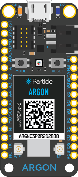 |  |
The Particle P2 module is the next generation Wi-Fi module from Particle. It is footprint compatible with our prior module, the P1, but is built on an upgraded chipset, supporting advanced features such as 5 GHz Wi-Fi, a 200MHz CPU, and built-in Bluetooth BLE 5.0.
| Feature | P2 | P1 | Photon | Argon |
|---|---|---|---|---|
| Style | SMD | SMD | Pin Module | Pin Module |
| Status LEDs | † | † | ✓ | ✓ |
| Reset and Mode Buttons | † | † | ✓ | ✓ |
| USB Connector | † | † | Micro B | Micro B |
| D7 Blue LED | ✓ | ✓ | ||
| LiPo Connector | ✓ | |||
| Battery Charger | ✓ | |||
| User application size | 2048 KB (2 MB) | 128 KB | 128KB | 256 KB |
| Flash file system1 | 2 MB | 2 MB | ||
| MCU | RTL8721DM | STM32F205RGY6 | STM32F205RGY6 | nRF52840 |
| Realtek Semiconductor | ST Microelectronics | ST Microelectronics | Nordic Semiconductor | |
| CPU | Cortex M33 @ 200 MHz | Cortex M3 @ 120 MHz | Cortex M3 @ 120 MHz | Cortex M3 @ 64 MHz |
| Cortex M23 @ 20 MHz | ||||
| RAM2 | 4608 KB | 128KB | 128 KB | 256 KB |
| Flash3 | 16 MB | 1 MB | 1 MB | 1 MB |
| Hardware FPU | ✓ | ✓ | ||
| Secure Boot | ✓ | |||
| Trust Zone | ✓ | } | ||
| } | ||||
| Wi-Fi | 802.11 a/b/g/n | 802.11 b/g/n | 802.11 b/g/n | 802.11 b/g/n |
| 2.4 GHz | ✓ | ✓ | ✓ | ✓ |
| 5 GHz | ✓ | |||
| Bluetooth | BLE 5.0 | BLE 5.0 | ||
| NFC Tag | External antenna required | |||
| Antenna | Shared for Wi-Fi and BLE | Wi-Fi only | Wi-Fi only | Separate Wi-Fi and BLE antennas |
| Built-in PCB antenna (Wi-Fi & BLE) | Built-in PCB antenna (Wi-Fi) | Built-in chip antenna (Wi-Fi) | Built-in chip antenna (BLE) | |
| Required external antenna (Wi-Fi) | ||||
| Optional external (Wi-Fi & BLE)4 | Optional external (Wi-Fi)4 | Optional external (Wi-Fi)4 | Optional external (BLE)4 | |
| Peripherals | USB 2.0 | USB 1.1 | USB 1.1 | USB 1.1 |
| Digital GPIO | 22 | 24 | 18 | 20 |
| Analog (ADC) | 6 | 13 | 8 | 6 |
| Analog (DAC) | 2 | 2 | ||
| UART | 1 | 2 | 26 | 1 |
| SPI | 2 | 2 | 2 | 2 |
| PWM | 6 | 12 | 9 | 8 |
| I2C | 1 | 1 | 1 | 1 |
| CAN | 1 | 1 | ||
| I2S | 15 | 15 | 1 | |
| JTAG | ✓ | ✓ | ||
| SWD | ✓ | ✓ | ✓ | ✓ |
† Optional but recommended. Add to your base board.
1A small amount of the flash file system is used by Device OS, most is available for user data storage using the POSIX filesystem API. This is separate from the flash memory used for Device OS, user application, and OTA transfers.
2 Total RAM; amount available to user applications is smaller. On the P2, available RAM is approximately 3072 KB. On the Argon, it is 80 KB. On the Photon, it is 55 KB.
3 Total built-in flash; amount available to user applications is smaller. The Argon also has a 4 MB external flash, a portion of which is available to user applications as a flash file system.
4 Onboard or external antenna is selectable in software.
5 The STM32 hardware supports I2S but there is no software support in Device OS or 3rd-party libraries.
6 The second UART on the Photon shares pins with the status LED, and requires unsoldering it (or its current limiting resistors) and using pads on the bottom of the module, making it impractical to use.
Hardware
Module style
The primary difference is that the Argon is a pin-based module that can be installed in solderless breadboard for prototyping, can be installed in a socket on your custom board, or soldered directly to your board.
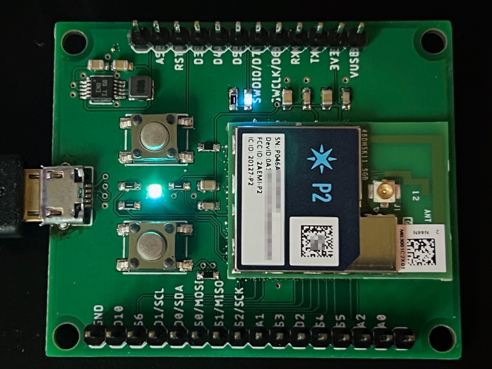
The P2 is only available as a SMD (surface mount device) that is typically reflow soldered to your base board. Your base board will need to be a custom printed circuit board, and cannot be a solderless breadboard or perforated prototyping board.
This can be done in small quantities by hand using a reflow oven or soldering hot plate. In quantity, it would be done by your PCBA (PCB with assembly) contractor.
This is a P2 custom board, not an actual product. Full instructions on how to build this board are included in the P2 First Board Tutorial.
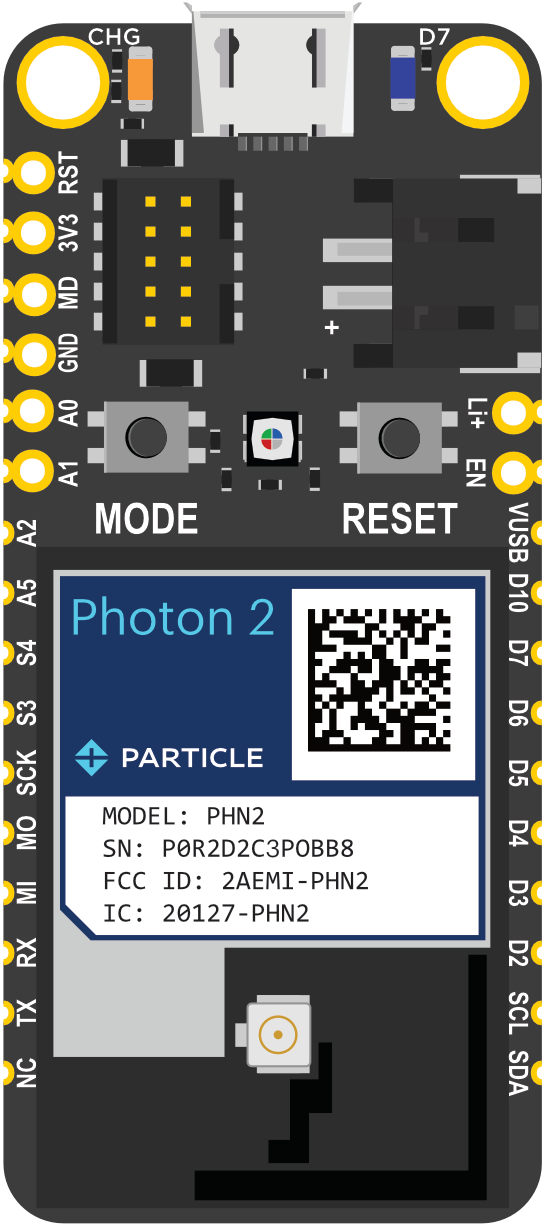
The Photon 2 is a pin-based module that contains a P2, and may be appropriate in many cases. If you are planning on scaling, it may be advantageous to migrate from the Argon directly to the P2 as you may require base board changes as there are some differences between the Argon and Photon 2.
The P2 reference design is a full breakout board with additional Feather sockets that are compatible with the Photon 2.
Status LED
The P2 does not include a status LED on the module. We recommend adding one to your base board.
Alternatively, if you have a separate hardware control panel, it provides the ability to put the RGB LED there and not duplicate it on the module or base board.
Device OS assumes a common anode RGB LED. One common LED that meets the requirements is the Cree CLMVC-FKA-CL1D1L71BB7C3C3 which is inexpensive and easily procured. You need to add three current limiting resistors. With this LED, we typically use 1K ohm current limiting resistors. These are much larger than necessary. They make the LED less blinding but still provide sufficient current to light the LEDs. If you want maximum brightness you should use the calculated values - 33 ohm on red, and 66 ohm on green and blue.
If you are using a different LED, you should limit current to 2mA per color.
A detailed explanation of different color codes of the RGB system LED can be found here.
Reset and Mode buttons
The P2 does not include buttons on module. We highly recommend including reset and mode buttons on your base board.
For example, you could use two-inexpensive SMD switches. The 4.5mm E-Switch TL3305AF160QG costs $0.20 in single quantities.
USB Connector
The P2 does not include a USB connector on the module. We recommend including one on your base board. This can be a USB Micro B, as on the Photon 2 and Argon, or you could use USB C.
Since you choose the connector you have the option of using a right-angle USB connector. This is handy if your board will be an enclosure where the board is recessed into the case under a removable cover. This can allow the USB connector to be accessed without removing the board from the enclosure.
| Part | Example | Price |
|---|---|---|
| USB micro B connector | Amphenol FCI 10118194-0001LF | $0.42 |
| CONN RCPT USB2.0 MICRO B SMD R/A | Amphenol FCI 10118194-0001LF | $0.42 |
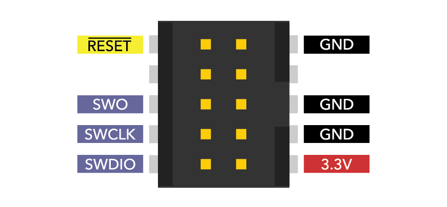
SWD/JTAG
The P2 does not include a SWD/JTAG debugging connector on the board. We recommend including the following pins available for debugging:
The Argon has dedicated pins for SWDIO and SWCLK and SWD remains running after your user firmware starts. On the Gen 2 and the P2, the SWD pins are shared with GPIO and by default SWD is disabled once the bootloader exits.
| Pin | Pin Name | Description | Interface | MCU |
|---|---|---|---|---|
| 1 | GND | Ground. Be sure you connect all P1 ground pins. | ||
| 34 | RST | Hardware reset. Pull low to reset; can leave unconnected in normal operation. | CHIP_EN | |
| 54 | D7 | D7 GPIO, SWDIO | SWDIO | PA[27] |
| 55 | D6 | D6 GPIO, SWCLK | SWCLK | PB[3] |
If you want to include the same 2x5 1.27mm connector as is on the Argon, this is one example of the connector:
| Description | Example | Price |
|---|---|---|
| CONN HEADER SMD 10POS 1.27MM | Samtec FTSH-105-01-F-DV-K | $3.91 |
Troubleshooting connector
In some cases, you may want to omit the reset and mode buttons, status LED, USB connector, and SWD/JTAG pins from your board board. If you do, we highly recommend adding a debug connector to make these features available for troubleshooting. The debug connector could be an actual connector, header pins, socket, card-edge connector, or SMD pads that allow an adapter or daughter card with these features.
Voltage regulator
The P2 requires regulated 3.3VDC at 500 mA. An voltage regulator is required on your base board if powering by USB (5V), LiPo (3.7V), or an external power source.
As of the first half of 2022, supply chain constraints are affecting the availability of voltage regulator components. There is no Device OS software dependency on the voltage regulator so you can choose any model as long as it meets the voltage and current requirements.
- This is often a switching regulator to save space, but this is not required.
- The Photon used a Richtek RT8008 (3.3V), which is hard to procure.
- The Argon used a Torex XCL223, which is no longer available. The pin compatible XCL224 is also no longer available.
- If the voltage is close to 3.3V, such as 5V USB, a linear regulator can be used.
The P2 requires more peak current and is more sensitive to power fluctuation than the Argon.
Power supply requirements:
- 3.3V output
- Maximum 5% voltage drop
- 100 mV peak-to-peak ripple maximum
- 500 mA minimum output current at 3.3V recommended for future compatibility
- Maintain these values at no-load as well as maximum load
In some cases, it may be necessary to add a supervisory/reset IC, such as the Richtek RT9818C or SG Micro SGM809-RXN3L/TR:
- If your power supply has a slew rate from 1.5V to 3.0V slower than 15 ms, a reset IC is required.
- If your power supply at power off cannot be guaranteed to drop below 0.3V before powering back up, a reset IC required.
See supervisory reset in the P2 datasheet, for additional information.
LiPo battery and li+ pin
The P2 does not include a LiPo battery connector or charging circuit on the module. If you want these features you will need to include them on your base board.
This is the LiPo battery connector used on the Argon:
| Description | Example | Price |
|---|---|---|
| JST-PH battery connector | JST B2B-PH-K-S-LF-SN | $0.17 |
As of the first half of 2022, supply chain constraints are affecting the supply of PMICs and charge controllers. Because of this, we are not recommending a specific model to use with your board.
The Argon uses a Torex XC6208A42 LiPo charge controller, however there is no need use this part and it will be difficult to obtain.
The Boron uses a full PMIC (bq24195) and fuel gauge (MAX17043). By including these features on your base board you can provide more full-featured operation on battery power than the Argon does.
EN pin
The Argon has the EN pin which can shut down the Torex XC9258 3.3V regulator to power down the 3.3V supply to the Argon nRF52840 MCU and the ESP32 Wi-Fi coprocessor.
This feature does not exist on the P2, however you could add equivalent circuitry on your base board. This could either be a regulator with power control like the Argon, or an external load switch like the Boron (Torex XC8107). The specific load switch is not important, as long as it meets the power requirements of the MCU and any additional peripherals on 3V3.
Pins A3, A4, and DAC (A6)
Pins A3, A4, DAC/A6 do not exist on the P2 and are NC.
You will need to use different pins if you are currently using these pins. There are a large number of additional pins (S0 - S6), however.
SPI
Both the Argon and P2 have two SPI ports, however the pins are different for both SPI ports. Also note that while pins D2 - D4 are used for SPI1 on both, the actual functions (SCK, MOSI, MISO) are on different pins!
The following are all SPI-related pins on the Argon and P2:
| Argon Pin Name | Argon SPI | P2 Pin Name | P2 SPI |
|---|---|---|---|
| A5 / D14 | SPI (SS) | A5 / D14 | |
| MISO / D11 | SPI (MISO) | A0 / D11 | |
| MOSI / D12 | SPI (MOSI) | A1 / D12 | |
| SCK / D13 | SPI (SCK) | A2 / D13 | |
| A2 / D17 | S2 / D17 | SPI (SCK) | |
| D2 | SPI1 (SCK) | D2 | SPI1 (MOSI) |
| D3 | SPI1 (MOSI) | D3 | SPI1 (MISO) |
| D4 | SPI1 (MISO) | D4 | SPI1 (SCK) |
| D5 | D5 | SPI1 (SS) | |
| S0 / D15 | SPI (MOSI) | ||
| S1 / D16 | SPI (MISO) | ||
| S3 / D18 | SPI (SS) |
If you are using SPI, Device OS 5.3.1 or later is recommended. Prior to that version, SPI ran at half of the set speed, and SPI1 ran at double the set speed. Timing has also been improved for large DMA transfers; prior to 5.3.1, there could be 1 µs gaps for every 16 bytes of data transferred.
SPI - Gen 3 devices (including Argon)
| SPI | SPI1 | |
|---|---|---|
| Maximum rate | 32 MHz | 32 MHz |
| Default rate | 16 MHz | 16 MHz |
| Clock | 64 MHz | 64 MHz |
- Available clock divisors: 2, 4, 8, 16, 32, 64, 128, 256
- Default divisor is 4
SPI - P2
| SPI | SPI1 | |
|---|---|---|
| Maximum rate | 25 MHz | 50 MHz |
| Hardware peripheral | RTL872x SPI1 | RTL872x SPI0 |
I2C
The P2 supports one I2C (two-wire serial interface) port on the same pins as the Argon (D0 and D1).
However on the P2, D0 is shared with A3 and D1 is shared with D4, so you cannot use A3 and A4 at the same time as I2C.
Also, the Argon supports a secondary I2C interface on D2 and D3; this is not supported on the P2.
| Argon Pin Name | Argon I2C | P2 Pin Name | P2 I2C |
|---|---|---|---|
| A3 / D16 | D0 / A3 | Wire (SDA) | |
| A4 / D15 | D1 / A4 | Wire (SCL) | |
| D0 | Wire (SDA) | D0 / A3 | Wire (SDA) |
| D1 | Wire (SCL) | D1 / A4 | Wire (SCL) |
| D2 | Wire1 (SDA) | D2 | |
| D3 | Wire1 (SCL) | D3 |
- On the P2 and Photon 2, the only valid I2C clock speeds are
CLOCK_SPEED_100KHZandCLOCK_SPEED_400KHZ. Other speeds are not supported at this time.
Serial (UART)
The primary UART serial (Serial1) is on the TX and RX pins on both the Argon and P2. On the Argon, hardware flow control (RTS/CTS) is available for Serial1 but this is not the case for the P2.
There is no secondary UART on the Argon, but there is one on the P2. The secondary UART Serial2 on the P2 does support hardware flow control.
If you are using Argon Serial1 with hardware flow control, you should switch to using Serial2 on the P2.
| Argon Pin Name | Argon Serial | P2 Pin Name | P2 Serial |
|---|---|---|---|
| A2 / D17 | S2 / D17 | Serial3 (RTS) | |
| D2 | Serial1 RTS | D2 | Serial2 (RTS) |
| D3 | Serial1 CTS | D3 | Serial2 (CTS) |
| D4 | D4 | Serial2 (TX) | |
| D5 | D5 | Serial2 (RX) | |
| RX / D10 | Serial1 RX | D10 / WKP | Serial3 (CTS) |
| RX / D9 | Serial1 (RX) | ||
| S0 / D15 | Serial3 (TX) | ||
| S1 / D16 | Serial3 (RX) | ||
| TX / D09 | Serial1 TX | TX / D8 | Serial1 (TX) |
| D8 / WKP | D10 / WKP | Serial3 (CTS) |
| Argon | P2 | |
|---|---|---|
| Buffer size | 64 bytes2 | 2048 bytes |
| 7-bit mode | ✓ | |
| 8-bit mode | ✓ | ✓ |
| 1 stop bit | ✓ | ✓ |
| 2 stop bits | ✓ | |
| No parity | ✓ | ✓ |
| Even parity | ✓ | ✓ |
| Odd parity | ✓ | |
| CTS/RTS flow control | ✓1 |
Supported Baud Rates:
| Baud Rate | Argon | P2 |
|---|---|---|
| 110 | ✓ | |
| 300 | ✓ | |
| 600 | ✓ | |
| 1200 | ✓ | ✓ |
| 2400 | ✓ | ✓ |
| 4800 | ✓ | ✓ |
| 9600 | ✓ | |
| 14400 | ✓ | |
| 19200 | ✓ | ✓ |
| 28800 | ✓ | ✓ |
| 38400 | ✓ | ✓ |
| 57600 | ✓ | ✓ |
| 76800 | ✓ | ✓ |
| 115200 | ✓ | ✓ |
| 128000 | ✓ | |
| 153600 | ✓ | |
| 230400 | ✓ | ✓ |
| 250000 | ✓ | |
| 380400 | ✓ | |
| 460800 | ✓ | |
| 460800 | ✓ | ✓ |
| 500000 | ✓ ✓ | |
| 921600 | ✓ | ✓ |
| 1000000 | ✓ | ✓ |
| 1382400 | ✓ | |
| 1444400 | ✓ | |
| 1500000 | ✓ | |
| 1843200 | ✓ | |
| 2000000 | ✓ | |
| 2100000 | ✓ | |
| 2764800 | ✓ | |
| 3000000 | ✓ | |
| 3250000 | ✓ | |
| 3692300 | ✓ | |
| 3750000 | ✓ | |
| 4000000 | ✓ | |
| 6000000 | ✓ |
1CTS/RTS flow control only on Serial2 and Serial3. It is optional.
2On the Argon, the buffer be resized larger in Device OS 3.2.0 and later.
Analog input (ADC)
For analog to digital conversion (ADC) using analogRead(), there are fewer ADC inputs on the P2:
| Argon Pin Name | Argon ADC | P2 Pin Name | P2 ADC |
|---|---|---|---|
| A1 / D18 | ✓ | A1 / D12 | ✓ |
| A3 / D16 | ✓ | D0 / A3 | ✓ |
| A4 / D15 | ✓ | D1 / A4 | ✓ |
| A5 / D14 | ✓ | A5 / D14 | ✓ |
| D0 | D0 / A3 | ✓ | |
| D1 | D1 / A4 | ✓ | |
| MISO / D11 | A0 / D11 | ✓ | |
| MOSI / D12 | A1 / D12 | ✓ | |
| SCK / D13 | A2 / D13 | ✓ | |
| A2 / D17 | ✓ | S2 / D17 | |
| A0 / D19 | ✓ | S4 / D19 |
On the P2, there are no pins A3 (hardware pin 21) and A4 (hardware pin 22); these are NC (no connection). However, P2 pin D0 (hardware pin 36) can be used as an analog input and has the alias A3. The same is true for P2 pin D1 (hardware pin 35), which has the alias A4.
The setADCSampleTime() function is not supported on the P2.
PWM (Pulse-width modulation)
The pins that support PWM are different on the Argon and P2.
| Argon Pin Name | Argon PWM | P2 Pin Name | P2 PWM |
|---|---|---|---|
| A1 / D18 | ✓ | A1 / D12 | |
| A3 / D16 | ✓ | D0 / A3 | |
| A4 / D15 | ✓ | D1 / A4 | ✓ |
| A5 / D14 | ✓ | A5 / D14 | ✓ |
| D1 | D1 / A4 | ✓ | |
| SCK / D13 | A2 / D13 | ✓ | |
| A2 / D17 | ✓ | S2 / D17 | |
| A0 / D19 | ✓ | S4 / D19 | |
| D2 | ✓ | D2 | |
| D3 | ✓ | D3 | |
| D4 | ✓ | D4 | |
| D5 | ✓ | D5 | |
| D6 | ✓ | D6 | |
| D7 | PWM is shared with the RGB LED, you can specify a different duty cycle but should not change the frequency. | D7 | |
| S0 / D15 | ✓ | ||
| S1 / D16 | ✓ | ||
| D8 / WKP | ✓ | D10 / WKP |
All available PWM pins on the P2 share a single timer. This means that they must all share a single frequency, but can have different duty cycles.
PDM
Pulse density modulation digital microphones can be used with the Microphone_PDM library and the P2, but only on specific pins. The Argon and Boron can use any pins for PDM (with the same library).
| Pin | Pin Name | Description | MCU |
|---|---|---|---|
| 43 | A1 / D12 | A1 Analog in, PDM DAT, GPIO | PB[2] |
| 50 | A0 / D11 | A0 Analog in, PDM CLK, GPIO | PB[1] |
I2S (Sound)
The Argon can use I2S via a 3rd-party library, however there has never been support for it in Device OS.
There is no software support for I2S on the P2, and while the RTL872x hardware supports I2S, the pins that it requires are in use by other ports.
BLE (Bluetooth LE)
BLE Central Mode on the P2 and Photon 2 is only supported in Device OS 5.1.0 and later. Earlier versions only supported BLE Peripheral Mode.
Sleep
The P2 can wake from STOP or ULTRA_LOW_POWER sleep mode on any GPIO, RISING, FALLING, or CHANGE.
The P2 can only wake from HIBERNATE sleep mode certain pins, RISING, FALLING, or CHANGE.
Pin D10 WKP is the same module pin location as the Argon pin D8, which is also the WKP pin. However, the Argon can wake from HIBERNATE on any GPIO, so if you use HIBERNATE mode with GPIO wake make sure the pin you have selected is compatible.
| Pin | Pin Name | Description | Interface | MCU |
|---|---|---|---|---|
| 30 | D10 / WKP | D10 GPIO, Serial 3 CTS, WKP. (Was WKP/A7 on P1.) | Pin can wake from HIBERNATE sleep | PA[15] |
| 40 | S0 / D15 | S0 GPIO, PWM, SPI MOSI, Serial3 TX, I2S MCLK. (Was P1S0 on P1.) | Pin can wake from HIBERNATE sleep | PA[12] |
| 41 | S1 / D16 | S1 GPIO, PWM, SPI MISO, Serial3 RX. (Was P1S1 on P1.) | Pin can wake from HIBERNATE sleep | PA[13] |
| 42 | S2 / D17 | S2 GPIO, SPI SCK, Serial3 RTS. (Was P1S2 on P1.) | Pin can wake from HIBERNATE sleep | PA[14] |
| 45 | D2 | D2 GPIO, Serial2 RTS, SPI1 MOSI | Pin can wake from HIBERNATE sleep | PA[16] |
| 51 | D3 | D3 GPIO, Serial2 CTS, SPI1 MISO | Pin can wake from HIBERNATE sleep | PA[17] |
| 52 | D4 | D4 GPIO, Serial2 TX, SPI1 SCK | Pin can wake from HIBERNATE sleep | PA[18] |
| 53 | D5 | D5 GPIO, Serial2 RX, SPI1 SS | Pin can wake from HIBERNATE sleep | PA[19] |
Internal pull-up or pull-down
Internal (MCU) pull-up and pull-down can be enabled using the pinMode() function and INPUT_PULLUP or INPUT_PULLDOWN.
- On the P2, the internal pull varies by pin and can be approximately 2.1K, 22K, or 42K.
- Pins A0, A1, D2, D3, D4, D5, D10, S0, S1, S2 are 2.1K
- Pins D0, D1, S4, S5, S6 are 22K
- Pins A2, A5, D6, TX, RX are 42K
- Pins S4, S5, S6 do not support pull-up or pull-down in HIBERNATE sleep mode. Use an external pull resistor if this is required.
- On the Argon (Gen 3), the internal pull is approximately 13K.
MODE button
The P2 MODE button does not have a hardware pull-up on it, so you must add an external pull-up (2.2K to 10K) to 3V3, or connect it to 3V3 if not using a button.
Interrupts
All pins can be used for interrupts on Gen 3 devices and the P2.
There is a limit of 8 pin interrupts on the Argon; this limitation does not exist on the P2.
Boot mode pins
These pins have a special function at boot. Beware when using these pins as input as they can trigger special modes in the MCU.
| Pin | Pin Name | Description | MCU |
|---|---|---|---|
| 54 | D7 | SWDIO. 40K pull-up at boot. Low at boot triggers MCU test mode. | PA[27] |
| 55 | D6 | SWCLK. 40K pull-down at boot. | PB[3] |
| 64 | TX / D8 | Low at boot triggers ISP flash download | PA[7] |
Battery voltage
The P2 does not include a LiPo battery connector, but if you connect your battery to VBAT_MEAS, you can measure the battery voltage as follows:
float voltage = analogRead(A6) / 819.2;
The constant is from the ADC range (0 - 4095) mapped to the voltage from 0 - 5 VDC (the maximum supported on VBAT_MEAS).
Note that battery voltage during discharge of a LiPo battery is not linear, so for battery powered applications where you need to know the state of charge, an external fuel gauge chip (such as the MAX17043 used on the Boron) is recommended.
Retained memory
The P2 and Photon 2 have limited support for retained memory, also referred to as Backup RAM or SRAM, in Device OS 5.3.1 and later.
Retained memory is preserved on RTL872x devices in the following cases:
| Case | Saved |
|---|---|
| When entering sleep modes | 5.3.1 and later |
| OTA firmware updates | 5.3.1 and later |
System.backupRamSync() |
5.3.1 and later |
System.reset() |
Not saved |
| Reset button or reset pin | Not saved |
| Every 10 seconds | 5.3.1 to 5.8.0 only |
Calling System.backupRamSync() will manually save the contents of retained memory to a dedicated flash page on the RTL872x processor and will be restored after the device is reset. You should avoid saving the data extremely frequently as it is slower than RAM and will cause flash wear and is relatively slow to execute.
Prior to Device OS 5.3.1, retained memory is not supported on RTL872x devices. The flash file system can be used, or you can use an external chip such as an I2C or SPI FRAM.
Retained memory is 3068 bytes.
Flash file system
Both the Argon and P2 have a 2 MB flash file system using the same POSIX API as Gen 3 devices. A small amount of space is reserved for system use including configuration data. Most of the space is available for user application use.
EEPROM
The EEPROM emulation API is the same across the Photon and P2.
Both the Argon and P2 have 4096 bytes of emulated EEPROM. On the P2 and Gen 3 devices, the EEPROM is actually just a file on the flash file system.
NFC tag
The Photon 2 does not have NFC Tag support. The Argon does.
Pin functions removed
The following pins served Argon-specific uses and are NC on the P2. You should not connect anything to these pins.
- Pins A3 and A4 on the P2 are shared with D0 and D1. You cannot use A3 and A4 at the same time as I2C (
Wire) on the P2.
| Pin Name | Description |
|---|---|
| EN | Power supply enable. Connect to GND to power down. Has internal weak (100K) pull-up. |
| LI+ | Connected to JST PH LiPo battery connector. 3.7V in or out. |
| VUSB | Power out (when powered by USB) 5 VDC at 1A maximum. Power in with limitations. |
Pin functions added
The following pins did not exist on the Argon but are available on the P2.
| Pin | Pin Name | Description |
|---|---|---|
| 5 | 3V3_IO | 3.3V power to MCU IO. |
| 2 | 3V3_RF | 3.3V power to RF module |
| 31 | RGBB | RGB LED Blue |
| 32 | RGBG | RGB LED Green |
| 29 | RGBR | RGB LED Red. Has 10K hardware pull-up. Do not hold low at boot. |
| 63 | RX / D9 | Serial1 RX (received data), GPIO |
| 40 | S0 / D15 | S0 GPIO, PWM, SPI MOSI, Serial3 TX, I2S MCLK. (Was P1S0 on P1.) |
| 41 | S1 / D16 | S1 GPIO, PWM, SPI MISO, Serial3 RX. (Was P1S1 on P1.) |
| 44 | S3 / D18 | S3 GPIO, I2S TX. (Was P1S3 on P1.), SPI SS |
| 48 | S5 / D20 | S5 GPIO, I2S CLK. (Was P1S5 on P1.) |
| 33 | S6 / D21 | S6 GPIO, I2S WS. (Was P1S6/TESTMODE on P1.) |
| 62 | USBDATA- | USB Data- |
| 61 | USBDATA+ | USB Data+ |
| 12 | VBAT_MEAS | Battery voltage measurement (optional). |
Recommended pin mappings
All-purpose mapping
This mapping is good for most situations. A3 and A4 cannot be used as ADC, but I2C, SPI, and Serial are mapped.
| Argon Pin Name | Argon Description | P2 Pin Name | P2 Description | P2 Pin Number | MCU |
|---|---|---|---|---|---|
| A0 / D19 | A0 Analog in, GPIO, PWM | A0 / D11 | A0 Analog in, PDM CLK, GPIO | 50 | PB[1] |
| A1 / D18 | A1 Analog in, GPIO, PWM | A1 / D12 | A1 Analog in, PDM DAT, GPIO | 43 | PB[2] |
| A2 / D17 | A2 Analog in, GPIO, PWM | A2 / D13 | A2 Analog in, PWM, GPIO | 49 | PB[7] |
| A3 / D16 | A3 Analog in, GPIO, PWM | S3 / D18 | S3 GPIO, I2S TX. (Was P1S3 on P1.), SPI SS | 44 | PB[26] |
| A4 / D15 | A4 Analog in, GPIO, PWM | S4 / D19 | S4 GPIO, I2S RX. (Was P1S4 on P1.) | 47 | PA[0] |
| A5 / D14 | A5 Analog in, GPIO, PWM, SPI SS | A5 / D14 | A5 Analog in, GPIO, PWM. | 23 | PB[4] |
| D0 | I2C SDA, GPIO | D0 / A3 | D0 GPIO, I2C SDA, A3 Analog In | 36 | PB[6] |
| D1 | I2C SCL, GPIO | D1 / A4 | D1 GPIO, PWM, I2C SCL, A4 Analog In | 35 | PB[5] |
| D2 | SPI1 SCK, Wire1 SDA, Serial1 RTS, PWM, GPIO | D2 | D2 GPIO, Serial2 RTS, SPI1 MOSI | 45 | PA[16] |
| D3 | SPI1 MOSI, Wire1 SCL, Serial1 CTS, PWM, GPIO | D3 | D3 GPIO, Serial2 CTS, SPI1 MISO | 51 | PA[17] |
| D4 | SPI1 MISO, PWM, GPIO | D4 | D4 GPIO, Serial2 TX, SPI1 SCK | 52 | PA[18] |
| D5 | PWM, GPIO | D5 | D5 GPIO, Serial2 RX, SPI1 SS | 53 | PA[19] |
| D6 | PWM, GPIO | D6 | D6 GPIO, SWCLK | 55 | PB[3] |
| D7 | PWM, GPIO | D7 | D7 GPIO, SWDIO | 54 | PA[27] |
| MISO / D11 | SPI MISO, GPIO | S1 / D16 | S1 GPIO, PWM, SPI MISO, Serial3 RX. (Was P1S1 on P1.) | 41 | PA[13] |
| MOSI / D12 | SPI MOSI, GPIO | S0 / D15 | S0 GPIO, PWM, SPI MOSI, Serial3 TX, I2S MCLK. (Was P1S0 on P1.) | 40 | PA[12] |
| RX / D10 | Serial RX, GPIO | RX / D9 | Serial1 RX (received data), GPIO | 63 | PA[8] |
| SCK / D13 | SPI SCK, GPIO | S2 / D17 | S2 GPIO, SPI SCK, Serial3 RTS. (Was P1S2 on P1.) | 42 | PA[14] |
| TX / D09 | Serial TX, GPIO | TX / D8 | Serial1 TX (transmitted data), GPIO | 64 | PA[7] |
SPI1 Preferred
If you need to use SPI1 on the D pins, this mapping is required. The D pins are ordered differently between the Argon and P2, and this affects SPI1.
| Argon Pin Name | Argon Description | P2 Pin Name | P2 Description | P2 Pin Number | MCU |
|---|---|---|---|---|---|
| A0 / D19 | A0 Analog in, GPIO, PWM | A0 / D11 | A0 Analog in, PDM CLK, GPIO | 50 | PB[1] |
| A1 / D18 | A1 Analog in, GPIO, PWM | A1 / D12 | A1 Analog in, PDM DAT, GPIO | 43 | PB[2] |
| A2 / D17 | A2 Analog in, GPIO, PWM | A2 / D13 | A2 Analog in, PWM, GPIO | 49 | PB[7] |
| A3 / D16 | A3 Analog in, GPIO, PWM | S3 / D18 | S3 GPIO, I2S TX. (Was P1S3 on P1.), SPI SS | 44 | PB[26] |
| A4 / D15 | A4 Analog in, GPIO, PWM | S4 / D19 | S4 GPIO, I2S RX. (Was P1S4 on P1.) | 47 | PA[0] |
| A5 / D14 | A5 Analog in, GPIO, PWM, SPI SS | A5 / D14 | A5 Analog in, GPIO, PWM. | 23 | PB[4] |
| D0 | I2C SDA, GPIO | D0 / A3 | D0 GPIO, I2C SDA, A3 Analog In | 36 | PB[6] |
| D1 | I2C SCL, GPIO | D1 / A4 | D1 GPIO, PWM, I2C SCL, A4 Analog In | 35 | PB[5] |
| D2 | SPI1 SCK, Wire1 SDA, Serial1 RTS, PWM, GPIO | D4 | D4 GPIO, Serial2 TX, SPI1 SCK | 52 | PA[18] |
| D3 | SPI1 MOSI, Wire1 SCL, Serial1 CTS, PWM, GPIO | D2 | D2 GPIO, Serial2 RTS, SPI1 MOSI | 45 | PA[16] |
| D4 | SPI1 MISO, PWM, GPIO | D3 | D3 GPIO, Serial2 CTS, SPI1 MISO | 51 | PA[17] |
| D5 | PWM, GPIO | D5 | D5 GPIO, Serial2 RX, SPI1 SS | 53 | PA[19] |
| D6 | PWM, GPIO | D6 | D6 GPIO, SWCLK | 55 | PB[3] |
| D7 | PWM, GPIO | D7 | D7 GPIO, SWDIO | 54 | PA[27] |
| MISO / D11 | SPI MISO, GPIO | S1 / D16 | S1 GPIO, PWM, SPI MISO, Serial3 RX. (Was P1S1 on P1.) | 41 | PA[13] |
| MOSI / D12 | SPI MOSI, GPIO | S0 / D15 | S0 GPIO, PWM, SPI MOSI, Serial3 TX, I2S MCLK. (Was P1S0 on P1.) | 40 | PA[12] |
| RX / D10 | Serial RX, GPIO | RX / D9 | Serial1 RX (received data), GPIO | 63 | PA[8] |
| SCK / D13 | SPI SCK, GPIO | S2 / D17 | S2 GPIO, SPI SCK, Serial3 RTS. (Was P1S2 on P1.) | 42 | PA[14] |
| TX / D09 | Serial TX, GPIO | TX / D8 | Serial1 TX (transmitted data), GPIO | 64 | PA[7] |
Full module pin comparison
3V3
| Argon | P2 | ||
|---|---|---|---|
| ∆ | Pin Number | 2 | 26 |
| Pin Name | 3V3 | 3V3 | |
| ∆ | Description | Regulated 3.3V DC output, maximum load 1000 mA | 3.3V power to MCU |
3V3_IO
| Added to P2 | |
|---|---|
| Pin Number | 5 |
| Pin Name | 3V3_IO |
| Description | 3.3V power to MCU IO. |
3V3_RF
| Added to P2 | |
|---|---|
| Pin Number | 2 |
| Pin Name | 3V3_RF |
| Description | 3.3V power to RF module |
A1
| Argon | P2 | ||
|---|---|---|---|
| ∆ | Pin Number | 6 | 43 |
| Pin Name | A1 | A1 | |
| ∆ | Pin Alternate Name | D18 | D12 |
| ∆ | Description | A1 Analog in, GPIO, PWM | A1 Analog in, PDM DAT, GPIO |
| Supports digitalRead | Yes | Yes | |
| Supports digitalWrite | Yes | Yes | |
| Supports analogRead | Yes | Yes | |
| ∆ | Supports analogWrite (PWM) | Yes | No |
| ∆ | Supports tone | A0, A1, A2, and A3 must have the same frequency. | No |
| ∆ | Supports attachInterrupt | Yes. You can only have 8 active interrupt pins. | Yes |
| ∆ | Internal pull resistance | 13K | 2.1K |
A3
| Argon | P2 | ||
|---|---|---|---|
| ∆ | Pin Number | 8 | 36 |
| ∆ | Pin Name | A3 | D0 |
| ∆ | Pin Alternate Name | D16 | A3 |
| ∆ | Description | A3 Analog in, GPIO, PWM | D0 GPIO, I2C SDA, A3 Analog In |
| Supports digitalRead | Yes | Yes | |
| Supports digitalWrite | Yes | Yes | |
| Supports analogRead | Yes | Yes | |
| ∆ | Supports analogWrite (PWM) | Yes | No |
| ∆ | Supports tone | A0, A1, A2, and A3 must have the same frequency. | No |
| ∆ | I2C interface | n/a | SDA. Use Wire object. Use 1.5K to 10K external pull-up resistor. |
| ∆ | Supports attachInterrupt | Yes. You can only have 8 active interrupt pins. | Yes |
| ∆ | Internal pull resistance | 13K | 22K |
A4
| Argon | P2 | ||
|---|---|---|---|
| ∆ | Pin Number | 9 | 35 |
| ∆ | Pin Name | A4 | D1 |
| ∆ | Pin Alternate Name | D15 | A4 |
| ∆ | Description | A4 Analog in, GPIO, PWM | D1 GPIO, PWM, I2C SCL, A4 Analog In |
| Supports digitalRead | Yes | Yes | |
| Supports digitalWrite | Yes | Yes | |
| Supports analogRead | Yes | Yes | |
| Supports analogWrite (PWM) | Yes | Yes | |
| ∆ | Supports tone | A4, A5, D2, and D3 must have the same frequency. | Yes |
| ∆ | I2C interface | n/a | SCL. Use Wire object. Use 1.5K to 10K external pull-up resistor. |
| ∆ | Supports attachInterrupt | Yes. You can only have 8 active interrupt pins. | Yes |
| ∆ | Internal pull resistance | 13K | 22K |
A5
| Argon | P2 | ||
|---|---|---|---|
| ∆ | Pin Number | 10 | 23 |
| Pin Name | A5 | A5 | |
| Pin Alternate Name | D14 | D14 | |
| ∆ | Description | A5 Analog in, GPIO, PWM, SPI SS | A5 Analog in, GPIO, PWM. |
| Supports digitalRead | Yes | Yes | |
| Supports digitalWrite | Yes | Yes | |
| Supports analogRead | Yes | Yes | |
| Supports analogWrite (PWM) | Yes | Yes | |
| ∆ | Supports tone | A4, A5, D2, and D3 must have the same frequency. | Yes |
| ∆ | SPI interface | SS. Use SPI object. This is only the default SS/CS pin, you can use any GPIO instead. | n/a |
| ∆ | Supports attachInterrupt | Yes. You can only have 8 active interrupt pins. | Yes |
| ∆ | Internal pull resistance | 13K | 42K |
D0
| Argon | P2 | ||
|---|---|---|---|
| ∆ | Pin Number | 16 | 36 |
| Pin Name | D0 | D0 | |
| ∆ | Pin Alternate Name | n/a | A3 |
| ∆ | Description | I2C SDA, GPIO | D0 GPIO, I2C SDA, A3 Analog In |
| Supports digitalRead | Yes | Yes | |
| Supports digitalWrite | Yes | Yes | |
| ∆ | Supports analogRead | No | Yes |
| ∆ | I2C interface | SDA. Use Wire object. | SDA. Use Wire object. Use 1.5K to 10K external pull-up resistor. |
| ∆ | Supports attachInterrupt | Yes. You can only have 8 active interrupt pins. | Yes |
| ∆ | Internal pull resistance | 13K | 22K |
D1
| Argon | P2 | ||
|---|---|---|---|
| ∆ | Pin Number | 17 | 35 |
| Pin Name | D1 | D1 | |
| ∆ | Pin Alternate Name | n/a | A4 |
| ∆ | Description | I2C SCL, GPIO | D1 GPIO, PWM, I2C SCL, A4 Analog In |
| Supports digitalRead | Yes | Yes | |
| Supports digitalWrite | Yes | Yes | |
| ∆ | Supports analogRead | No | Yes |
| ∆ | Supports analogWrite (PWM) | No | Yes |
| ∆ | Supports tone | No | Yes |
| ∆ | I2C interface | SCL. Use Wire object. | SCL. Use Wire object. Use 1.5K to 10K external pull-up resistor. |
| ∆ | Supports attachInterrupt | Yes. You can only have 8 active interrupt pins. | Yes |
| ∆ | Internal pull resistance | 13K | 22K |
D11
| Argon | P2 | ||
|---|---|---|---|
| ∆ | Pin Number | 13 | 50 |
| ∆ | Pin Name | MISO | A0 |
| Pin Alternate Name | D11 | D11 | |
| ∆ | Description | SPI MISO, GPIO | A0 Analog in, PDM CLK, GPIO |
| Supports digitalRead | Yes | Yes | |
| Supports digitalWrite | Yes | Yes | |
| ∆ | Supports analogRead | No | Yes |
| ∆ | SPI interface | MISO. Use SPI object. | n/a |
| ∆ | Supports attachInterrupt | Yes. You can only have 8 active interrupt pins. | Yes |
| ∆ | Internal pull resistance | 13K | 2.1K |
D12
| Argon | P2 | ||
|---|---|---|---|
| ∆ | Pin Number | 12 | 43 |
| ∆ | Pin Name | MOSI | A1 |
| Pin Alternate Name | D12 | D12 | |
| ∆ | Description | SPI MOSI, GPIO | A1 Analog in, PDM DAT, GPIO |
| Supports digitalRead | Yes | Yes | |
| Supports digitalWrite | Yes | Yes | |
| ∆ | Supports analogRead | No | Yes |
| ∆ | SPI interface | MOSI. Use SPI object. | n/a |
| ∆ | Supports attachInterrupt | Yes. You can only have 8 active interrupt pins. | Yes |
| ∆ | Internal pull resistance | 13K | 2.1K |
D13
| Argon | P2 | ||
|---|---|---|---|
| ∆ | Pin Number | 11 | 49 |
| ∆ | Pin Name | SCK | A2 |
| Pin Alternate Name | D13 | D13 | |
| ∆ | Description | SPI SCK, GPIO | A2 Analog in, PWM, GPIO |
| Supports digitalRead | Yes | Yes | |
| Supports digitalWrite | Yes | Yes | |
| ∆ | Supports analogRead | No | Yes |
| ∆ | Supports analogWrite (PWM) | No | Yes |
| ∆ | Supports tone | No | Yes |
| ∆ | SPI interface | SCK. Use SPI object. | n/a |
| ∆ | Supports attachInterrupt | Yes. You can only have 8 active interrupt pins. | Yes |
| ∆ | Internal pull resistance | 13K | 42K |
D17
| Argon | P2 | ||
|---|---|---|---|
| ∆ | Pin Number | 7 | 42 |
| ∆ | Pin Name | A2 | S2 |
| Pin Alternate Name | D17 | D17 | |
| ∆ | Description | A2 Analog in, GPIO, PWM | S2 GPIO, SPI SCK, Serial3 RTS. (Was P1S2 on P1.) |
| Supports digitalRead | Yes | Yes | |
| Supports digitalWrite | Yes | Yes | |
| ∆ | Supports analogRead | Yes | No |
| ∆ | Supports analogWrite (PWM) | Yes | No |
| ∆ | Supports tone | A0, A1, A2, and A3 must have the same frequency. | No |
| ∆ | UART serial | n/a | RTS. Use Serial3 object. Flow control optional. |
| ∆ | SPI interface | n/a | SCK. Use SPI object. |
| ∆ | Supports attachInterrupt | Yes. You can only have 8 active interrupt pins. | Yes |
| ∆ | Internal pull resistance | 13K | 2.1K |
D19
| Argon | P2 | ||
|---|---|---|---|
| ∆ | Pin Number | 5 | 47 |
| ∆ | Pin Name | A0 | S4 |
| Pin Alternate Name | D19 | D19 | |
| ∆ | Description | A0 Analog in, GPIO, PWM | S4 GPIO, I2S RX. (Was P1S4 on P1.) |
| Supports digitalRead | Yes | Yes | |
| Supports digitalWrite | Yes | Yes | |
| ∆ | Supports analogRead | Yes | No |
| ∆ | Supports analogWrite (PWM) | Yes | No |
| ∆ | Supports tone | A0, A1, A2, and A3 must have the same frequency. | No |
| ∆ | Supports attachInterrupt | Yes. You can only have 8 active interrupt pins. | Yes |
| ∆ | I2S interface | n/a | I2S RX |
| ∆ | Internal pull resistance | 13K | 22K. No internal pull up or pull down in HIBERNATE sleep mode. |
D2
| Argon | P2 | ||
|---|---|---|---|
| ∆ | Pin Number | 18 | 45 |
| Pin Name | D2 | D2 | |
| ∆ | Description | SPI1 SCK, Wire1 SDA, Serial1 RTS, PWM, GPIO | D2 GPIO, Serial2 RTS, SPI1 MOSI |
| Supports digitalRead | Yes | Yes | |
| Supports digitalWrite | Yes | Yes | |
| ∆ | Supports analogWrite (PWM) | Yes | No |
| ∆ | Supports tone | A4, A5, D2, and D3 must have the same frequency. | No |
| ∆ | UART serial | Options RTS hardware flow control for Serial1 | RTS. Use Serial2 object. Flow control optional. |
| ∆ | SPI interface | SCK. Use SPI1 object. | MOSI. Use SPI1 object. |
| ∆ | I2C interface | SDA. Use Wire1 object. | n/a |
| ∆ | Supports attachInterrupt | Yes. You can only have 8 active interrupt pins. | Yes |
| ∆ | Internal pull resistance | 13K | 2.1K |
D3
| Argon | P2 | ||
|---|---|---|---|
| ∆ | Pin Number | 19 | 51 |
| Pin Name | D3 | D3 | |
| ∆ | Description | SPI1 MOSI, Wire1 SCL, Serial1 CTS, PWM, GPIO | D3 GPIO, Serial2 CTS, SPI1 MISO |
| Supports digitalRead | Yes | Yes | |
| Supports digitalWrite | Yes | Yes | |
| ∆ | Supports analogWrite (PWM) | Yes | No |
| ∆ | Supports tone | A4, A5, D2, and D3 must have the same frequency. | No |
| ∆ | UART serial | Options CTS hardware flow control for Serial1 | CTS. Use Serial2 object. Flow control optional. |
| ∆ | SPI interface | MOSI. Use SPI1 object. | MISO. Use SPI1 object. |
| ∆ | I2C interface | SCL. Use Wire1 object. | n/a |
| ∆ | Supports attachInterrupt | Yes. You can only have 8 active interrupt pins. | Yes |
| ∆ | Internal pull resistance | 13K | 2.1K |
D4
| Argon | P2 | ||
|---|---|---|---|
| ∆ | Pin Number | 20 | 52 |
| Pin Name | D4 | D4 | |
| ∆ | Description | SPI1 MISO, PWM, GPIO | D4 GPIO, Serial2 TX, SPI1 SCK |
| Supports digitalRead | Yes | Yes | |
| Supports digitalWrite | Yes | Yes | |
| ∆ | Supports analogWrite (PWM) | Yes | No |
| ∆ | Supports tone | D4, D5, D6, and D7 must have the same frequency. | No |
| ∆ | UART serial | n/a | TX. Use Serial2 object. |
| ∆ | SPI interface | MISO. Use SPI1 object. | SCK. Use SPI1 object. |
| ∆ | Supports attachInterrupt | Yes. You can only have 8 active interrupt pins. | Yes |
| ∆ | Internal pull resistance | 13K | 2.1K |
D5
| Argon | P2 | ||
|---|---|---|---|
| ∆ | Pin Number | 21 | 53 |
| Pin Name | D5 | D5 | |
| ∆ | Description | PWM, GPIO | D5 GPIO, Serial2 RX, SPI1 SS |
| Supports digitalRead | Yes | Yes | |
| Supports digitalWrite | Yes | Yes | |
| ∆ | Supports analogWrite (PWM) | Yes | No |
| ∆ | Supports tone | D4, D5, D6, and D7 must have the same frequency. | No |
| ∆ | UART serial | n/a | RX. Use Serial2 object. |
| ∆ | SPI interface | n/a | SS. Use SPI1 object. Can use any pin for SPI1 SS/CS however. |
| ∆ | Supports attachInterrupt | Yes. You can only have 8 active interrupt pins. | Yes |
| ∆ | Internal pull resistance | 13K | 2.1K |
D6
| Argon | P2 | ||
|---|---|---|---|
| ∆ | Pin Number | 22 | 55 |
| Pin Name | D6 | D6 | |
| ∆ | Description | PWM, GPIO | D6 GPIO, SWCLK |
| Supports digitalRead | Yes | Yes | |
| Supports digitalWrite | Yes | Yes | |
| ∆ | Supports analogWrite (PWM) | Yes | No |
| ∆ | Supports tone | D4, D5, D6, and D7 must have the same frequency. | No |
| ∆ | Supports attachInterrupt | Yes. You can only have 8 active interrupt pins. | Yes |
| ∆ | Internal pull resistance | 13K | 42K |
| ∆ | SWD interface | n/a | SWCLK. 40K pull-down at boot. |
| ∆ | Signal used at boot | n/a | SWCLK. 40K pull-down at boot. |
D7
| Argon | P2 | ||
|---|---|---|---|
| ∆ | Pin Number | 23 | 54 |
| Pin Name | D7 | D7 | |
| ∆ | Description | PWM, GPIO | D7 GPIO, SWDIO |
| ∆ | Supports digitalRead | Yes | Yes. |
| ∆ | Supports digitalWrite | Yes | Yes. On the Photon this is the blue D7 LED. |
| ∆ | Supports analogWrite (PWM) | PWM is shared with the RGB LED, you can specify a different duty cycle but should not change the frequency. | No |
| ∆ | Supports attachInterrupt | Yes. You can only have 8 active interrupt pins. | Yes |
| ∆ | Internal pull resistance | 13K | 42K |
| ∆ | SWD interface | n/a | SWDIO. 40K pull-up at boot. |
| ∆ | Signal used at boot | n/a | SWDIO. 40K pull-up at boot. Low at boot triggers MCU test mode. |
EN
| Removed from Argon | |
|---|---|
| Pin Number | 26 |
| Pin Name | EN |
| Description | Power supply enable. Connect to GND to power down. Has internal weak (100K) pull-up. |
GND
| Argon | P2 | ||
|---|---|---|---|
| ∆ | Pin Number | 4 | 1 |
| Pin Name | GND | GND | |
| ∆ | Description | Ground. | Ground. Be sure you connect all P1 ground pins. |
LI+
| Removed from Argon | |
|---|---|
| Pin Number | 27 |
| Pin Name | LI+ |
| Description | Connected to JST PH LiPo battery connector. 3.7V in or out. |
MODE
| Argon | P2 | ||
|---|---|---|---|
| ∆ | Pin Number | 3 | 46 |
| Pin Name | MODE | MODE | |
| ∆ | Pin Alternate Name | D20 | n/a |
| ∆ | Description | MODE button, has internal pull-up | MODE button. Pin number constant is BTN. External pull-up required! |
| ∆ | Supports attachInterrupt | n/a | Yes |
NC
| Added to P2 | |
|---|---|
| Pin Number | 7 |
| Pin Name | NC |
| Description | No connection. Do not connect anything to this pin. |
RGBB
| Added to P2 | |
|---|---|
| Pin Number | 31 |
| Pin Name | RGBB |
| Description | RGB LED Blue |
| Supports attachInterrupt | Yes |
RGBG
| Added to P2 | |
|---|---|
| Pin Number | 32 |
| Pin Name | RGBG |
| Description | RGB LED Green |
| Supports attachInterrupt | Yes |
RGBR
| Added to P2 | |
|---|---|
| Pin Number | 29 |
| Pin Name | RGBR |
| Description | RGB LED Red. Has 10K hardware pull-up. Do not hold low at boot. |
| Supports attachInterrupt | Yes |
RST
| Argon | P2 | ||
|---|---|---|---|
| ∆ | Pin Number | 1 | 34 |
| Pin Name | RST | RST | |
| Description | Hardware reset. Pull low to reset; can leave unconnected in normal operation. | Hardware reset. Pull low to reset; can leave unconnected in normal operation. |
RX
| Argon | P2 | ||
|---|---|---|---|
| ∆ | Pin Number | 14 | 30 |
| ∆ | Pin Name | RX | D10 |
| ∆ | Pin Alternate Name | D10 | WKP |
| ∆ | Description | Serial RX, GPIO | D10 GPIO, Serial 3 CTS, WKP. (Was WKP/A7 on P1.) |
| Supports digitalRead | Yes | Yes | |
| Supports digitalWrite | Yes | Yes | |
| ∆ | UART serial | RX. Use Serial1 object. | CTS. Use Serial3 object. Flow control optional. |
| ∆ | Supports attachInterrupt | Yes. You can only have 8 active interrupt pins. | Yes |
| ∆ | Internal pull resistance | 13K | 2.1K |
RX
| Added to P2 | |
|---|---|
| Pin Number | 63 |
| Pin Name | RX |
| Pin Alternate Name | D9 |
| Description | Serial1 RX (received data), GPIO |
| Supports digitalRead | Yes |
| Supports digitalWrite | Yes |
| UART serial | RX. Use Serial1 object. |
| Supports attachInterrupt | Yes |
| Internal pull resistance | 42K |
S0
| Added to P2 | |
|---|---|
| Pin Number | 40 |
| Pin Name | S0 |
| Pin Alternate Name | D15 |
| Description | S0 GPIO, PWM, SPI MOSI, Serial3 TX, I2S MCLK. (Was P1S0 on P1.) |
| Supports digitalRead | Yes |
| Supports digitalWrite | Yes |
| Supports analogWrite (PWM) | Yes |
| Supports tone | Yes |
| UART serial | TX. Use Serial3 object. |
| SPI interface | MOSI. Use SPI object. |
| Supports attachInterrupt | Yes |
| I2S interface | I2S MCLK |
| Internal pull resistance | 2.1K |
S1
| Added to P2 | |
|---|---|
| Pin Number | 41 |
| Pin Name | S1 |
| Pin Alternate Name | D16 |
| Description | S1 GPIO, PWM, SPI MISO, Serial3 RX. (Was P1S1 on P1.) |
| Supports digitalRead | Yes |
| Supports digitalWrite | Yes |
| Supports analogWrite (PWM) | Yes |
| Supports tone | Yes |
| UART serial | RX. Use Serial3 object. |
| SPI interface | MISO. Use SPI object. |
| Supports attachInterrupt | Yes |
| Internal pull resistance | 2.1K |
S3
| Added to P2 | |
|---|---|
| Pin Number | 44 |
| Pin Name | S3 |
| Pin Alternate Name | D18 |
| Description | S3 GPIO, I2S TX. (Was P1S3 on P1.), SPI SS |
| Supports digitalRead | Yes |
| Supports digitalWrite | Yes |
| SPI interface | Default SS for SPI. |
| Supports attachInterrupt | Yes |
| I2S interface | I2S TX |
| Internal pull resistance | 2.1K |
S5
| Added to P2 | |
|---|---|
| Pin Number | 48 |
| Pin Name | S5 |
| Pin Alternate Name | D20 |
| Description | S5 GPIO, I2S CLK. (Was P1S5 on P1.) |
| Supports digitalWrite | Yes |
| Supports attachInterrupt | Yes |
| I2S interface | I2S CLK |
| Internal pull resistance | 22K. No internal pull up or pull down in HIBERNATE sleep mode |
S6
| Added to P2 | |
|---|---|
| Pin Number | 33 |
| Pin Name | S6 |
| Pin Alternate Name | D21 |
| Description | S6 GPIO, I2S WS. (Was P1S6/TESTMODE on P1.) |
| Supports digitalRead | Yes |
| Supports digitalWrite | Yes |
| Supports attachInterrupt | Yes |
| I2S interface | I2S WS |
| Internal pull resistance | 22K. No internal pull up or pull down in HIBERNATE sleep mode. |
TX
| Argon | P2 | ||
|---|---|---|---|
| ∆ | Pin Number | 15 | 64 |
| Pin Name | TX | TX | |
| ∆ | Pin Alternate Name | D09 | D8 |
| ∆ | Description | Serial TX, GPIO | Serial1 TX (transmitted data), GPIO |
| Supports digitalRead | Yes | Yes | |
| Supports digitalWrite | Yes | Yes | |
| UART serial | TX. Use Serial1 object. | TX. Use Serial1 object. | |
| ∆ | Supports attachInterrupt | Yes. You can only have 8 active interrupt pins. | Yes |
| ∆ | Internal pull resistance | 13K | 42K |
| ∆ | Signal used at boot | n/a | Low at boot triggers ISP flash download |
USBDATA-
| Added to P2 | |
|---|---|
| Pin Number | 62 |
| Pin Name | USBDATA- |
| Description | USB Data- |
| Input is 5V Tolerant | Yes |
USBDATA+
| Added to P2 | |
|---|---|
| Pin Number | 61 |
| Pin Name | USBDATA+ |
| Description | USB Data+ |
| Input is 5V Tolerant | Yes |
VBAT_MEAS
| Added to P2 | |
|---|---|
| Pin Number | 12 |
| Pin Name | VBAT_MEAS |
| Description | Battery voltage measurement (optional). |
| Input is 5V Tolerant | Yes |
VUSB
| Removed from Argon | |
|---|---|
| Pin Number | 25 |
| Pin Name | VUSB |
| Description | Power out (when powered by USB) 5 VDC at 1A maximum. Power in with limitations. |
| Input is 5V Tolerant | Yes |
WKP
| Argon | P2 | ||
|---|---|---|---|
| ∆ | Pin Number | 24 | 30 |
| ∆ | Pin Name | D8 | D10 |
| Pin Alternate Name | WKP | WKP | |
| ∆ | Description | GPIO, PWM | D10 GPIO, Serial 3 CTS, WKP. (Was WKP/A7 on P1.) |
| Supports digitalRead | Yes | Yes | |
| Supports digitalWrite | Yes | Yes | |
| ∆ | Supports analogWrite (PWM) | Yes | No |
| ∆ | Supports tone | D4, D5, D6, and D7 must have the same frequency. | No |
| ∆ | UART serial | n/a | CTS. Use Serial3 object. Flow control optional. |
| ∆ | Supports attachInterrupt | Yes. You can only have 8 active interrupt pins. | Yes |
| ∆ | Internal pull resistance | 13K | 2.1K |
Software
Wi-Fi Configuration
The P2 and Argon utilize BLE or USB for configuration of Wi-Fi rather than the SoftAP approach taken with the P1. Wi-Fi setup for the P2 should be very similar to the Argon.
| Feature | P2 | P1 | Argon |
|---|---|---|---|
| Wi-Fi (SoftAP) | ✓ | ||
| BLE | ✓ | ✓ |
User firmware binary size
One major advantage of the P2 is that user firmware binaries can be up to 2048 Kbytes.
On the Argon (Device OS 3.1 and later), it's 256 Kbytes, or 128 Kbytes for older version of Device OS.
Platform ID
The Platform ID of the P2 (32, PLATFORM_P2) is different from that of the Argon (12) because of the vastly different hardware.
If you have a product based on the Argon, you will need to create a separate product for devices using the P2. While you may be able to use the same source code to build your application, the firmware binaries uploaded to the console will be different, so they need to be separate products. This generally does not affect billing as only the number of devices, not the number of products, is counted toward your plan limits.
Third-party libraries
Most third-party libraries are believed to be compatible. The exceptions include:
- Libraries for MCU-specific features (such as ADC DMA)
- Libraries that are hardcoded to support only certain platforms by their PLATFORM_ID
- Libraries that manipulate GPIO at high speeds or are timing-dependent
DS18B20 (1-Wire temperature sensor)
- Not compatible
- OneWire library requires high-speed GPIO support
- Can use DS2482 I2C to 1-Wire bridge chip instead
- SHT30 sensors (I2C) may be an alternative in some applications
FastLED
- Not compatible.
- In theory the library could be modified to use the same technique as the NeoPixel library.
NeoPixel (WS2812, WS2812B, and WS2813)
- Requires Device OS 5.3.2 or later and Particle-NeoPixel version 1.0.3.
OneWire
- Not compatible
- OneWire library requires high-speed GPIO support
- Can use DS2482 I2C to OneWire bridge instead
DHT22 and DHT11 (temperature and humidity sensor)
- Not compatible, requires high-speed GPIO support
- Using an I2C temperature and humidity sensor like the SHT3x is recommended instead
SHT1x (temperature and humidity sensor)
- Not compatible, requires high-speed GPIO support
- SHT3x using I2C is recommended
SparkIntervalTimer
- Not compatible at this time
- Requires hardware timer support from user firmware
Version history
| Revision | Date | Author | Comments |
|---|---|---|---|
| pre | 2022-04-06 | RK | Pre-release |
| 2022-04-08 | RK | Added recommended pin mappings | |
| 2022-04-12 | RK | Added serial baud rates | |
| 2022-07-14 | RK | No hardware pull-up on MODE pin | |
| 2022-07-18 | RK | List which pins have which pull-up or pull-down value | |
| 2022-08-12 | RK | Warning about BLE central mode not available | |
| 2022-10-05 | RK | Added HIBERNATE sleep section | |
| 2022-11-17 | RK | Pin D0 does not have PWM | |
| 001 | 2023-03-13 | RK | Removed preliminary banner |
| 002 | 2023-04-05 | RK | Added Device OS 5.3.1 information for SPI and retained memory |
| 003 | 2023-04-24 | RK | Document VBAT_MEAS and CHG |
| 004 | 2023-05-05 | RK | Fix available RAM |
| 005 | 2024-03-11 | RK | Photon 2 has a USB Micro B, not USB C |
| 006 | 2024-03-15 | RK | The UART baud rate 2400, 4800, 380400, 460800 are supported but were not listed |
| 007 | 2024-04-18 | RK | Add PDM microphone |
| 008 | 2025-01-07 | RK | Added power supply notes |