
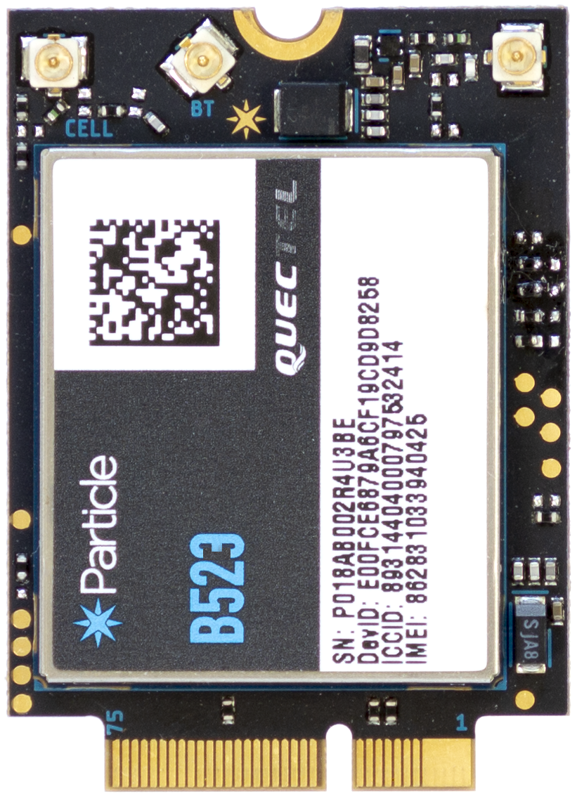
B524/B523 datasheet
Functional description
Overview
The B-Series System-on-a-Module (SoM) is a LTE Cat 1 cellular device with support for BLE (Bluetooth LE). It is based on the Nordic nRF52840 microcontroller.
The B-Series is designed to be integrated into your circuit board design, plugging into a M.2 NGFF connector on your board, allowing the module to be changed or upgraded easily.
Features
Features - B524
- Quectel EG91-E modem
- LTE category 1 module for EMEAA region
- 3GPP E-UTRA Release 13
- Cat 1 bands supported: 1, 3, 7, 8, 20, 28A
- 2G and 3G fallback (900, 1800, and 2100 MHz)
- Embedded Particle EtherSIM (B524)
- Support for selected countries in Europe, Middle East, Africa, and Asia, including Australia and New Zealand. See the cellular carrier list for more information.
Features - B523
- Quectel EG91-E modem
- LTE category 1 module for EMEAA region
- 3GPP E-UTRA Release 13
- Cat 1 bands supported: 1, 3, 7, 8, 20, 28A
- 2G and 3G fallback (900, 1800, and 2100 MHz)
- Embedded Particle SIM (B523)
- Support for Europe only
Features - all models
- Nordic Semiconductor nRF52840 SoC
- ARM Cortex-M4F 32-bit processor @ 64MHz
- 1MB flash, 256KB RAM
- Bluetooth 5: 2 Mbps, 1 Mbps, 500 Kbps, 125 Kbps
- Supports DSP instructions, HW accelerated Floating Point Unit (FPU) and encryption functions
- Up to +8 dBm TX power (down to -20 dBm in 4 dB steps)
- NFC-A tag
- On-module additional 8MB SPI flash
- 24 mixed signal GPIO (8 x Analog, 8 x PWM), UART, I2C, SPI
- USB 2.0 full speed (12 Mbps)
- JTAG (SWD) pins
- Pins for RGB LED used for connection status
- Pins for reset and mode buttons
- On-module MFF2 Particle SIM
- Two on-module U.FL connectors for external antennas
- M.2 interface
- CE certified
- RoHS compliant (lead-free)
Model comparison
| B404X | B404 | B402 | B524 | B523 | B504e | |
|---|---|---|---|---|---|---|
| Region | NorAm | NorAm | NorAm | EMEAA | Europe | Americas |
| EtherSIM | ✓ | ✓ | ✓ | ✓ | ||
| Supply Secure | ✓ | ✓ | ✓ | |||
| Lowest power (LTE Cat M1) | ✓ | ✓ | ✓ | |||
| Fastest speed (LTE Cat 1) | ✓ | ✓ | ✓ | |||
| Cellular fallback | 3G, 2G | 3G, 2G | 3G | |||
| Lifecycle | GA | NRND | Deprecated | GA | Deprecated | In development |
- EtherSIM devices generally have a larger number of carriers and more may be added in the future
- NorAm: North America (United States, Canada, and Mexico)
- Americas: North America, Central, and South America (not all countries supported)
- LTE Cat M1: Low-power cellular intended for IoT devices
- LTE Cat 1: Available in more countries and has higher data rates
- EMEAA: Europe, Middle East, Africa, and Asia (not all countries supported)
- NRND: Not recommended for new designs
- See the Carrier list for specific carrier and country compatibility
- See the Supply secure FAQ for more information
- See Lifestyle stages for more information
Device OS support
It is recommended that you use the latest version in the 4.x LTS release line with the B524 and B523.
The B524 and B523 are compatible with Device OS 2.x LTS, however the 2.x LTS release line is in the Extended Support and Maintenance (ESM) window and will stop being supported in 2024.
For information on upgrading Device OS, see Version information. For the latest version shipped from the factory, see Manufacturing firmware versions page. See also Long Term Support (LTS) releases.
Interfaces
Block diagram
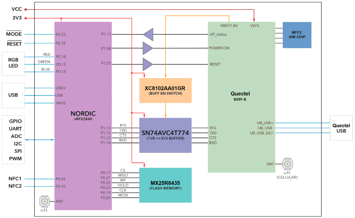
Power
VCC
VCC is used to supply power to the Quectel EG91-E cellular module. The recommended input voltage range on this pin is between 3.6V to 4.2V DC. This can be connected directly to a 3.7V LiPo battery. Make sure that the supply can handle currents of at least 2 A.
If you are not using a battery, or using a battery of a different voltage, you should use a regulator to supply 3.7V to 4.2V at 2A. You may want to add additional bulk capacitors to handle the short, high current peak usage when the cellular modem is transmitting.
3V3
3V3 is used to supply power to nRF52840, logic ICs, memory, etc.. The 3V3 input voltage range is between 3V to 3.6V DC, but 3.3V is recommended. Make sure that the supply can handle a minimum of 150 mA, however we recommend a minimum of 500 mA supplied from your base board to allow for compatibility with future modules.
These limits do not include any 3.3V peripherals on your base board, so that may increase the current requirements.
Power supply requirements:
- 3.3V output
- Maximum 5% voltage drop
- 100 mV peak-to-peak ripple maximum
- 500 mA minimum output current at 3.3V recommended for future compatibility
- Maintain these values at no-load as well as maximum load
We do not recommend using a single 3.6V supply for both VCC and 3V3 as the cellular modem performance may be lower below 3.7V. Use two separate regulators for best results.
VBus
VBus is connected to the USB detect pin of nRF52840 to enables the USB interface. The recommended input voltage range is between 4.35V to 5.5V DC.
Antenna
There are two radios on the B523 module. A BLE radio (nRF52840) and a cellular radio (Quectel). We have provided two u.FL connectors to plug in the cellular and BLE antenna. These are required if you wish to use the cellular and BLE. If you do not need BLE, you do not need to connect the BLE antenna.
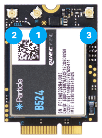
| Number | Label | Purpose |
|---|---|---|
| 1 | BT | Bluetooth antenna (optional) |
| 2 | CELL | Quectel cellular modem antenna |
| 3 | ANT_DIV | LTE cellular receive diversity antenna |
The third connector is the LTE cellular receive diversity antenna. A second cellular antenna can be connected to this connector to improve performance when the device will be moving at high speeds. It is only used for LTE Cat 1 connections and is not supported when in 2G or 3G mode. This antenna is not necessary in most cases and is not included in evaluation kits. (The B402 does not have this connector as receive diversity is not supported in LTE Cat M1 mode.)
Certified cellular antenna
| SKU | Description |
|---|---|
| ANTCW2EA | Particle Cellular Flex Antenna 2G/3G/LTE [x1] |
| ANTCW2TY | Particle Cellular Flex Antenna 2G/3G/LTE Tray of 50 [x50] |
- Type: LTE Ultra Wide Band Flex Antenna
- Frequency/band: 698 MHz-2690 MHz
- RoHS Compliant
- Mechanical Specs:
- Dimensions: 97 x 21 x 0.2 mm
- Mounting: 3M adhesive backed for application on non-metallic surfaces
- Connector type: FPC + IPEX connector
- Cable length: 210 mm
- Gain: 4.71 dBi
Particle devices are certified for use only with the designated antenna specified above. The use of alternative antennas with our modules could necessitate a recertification process. To fully understand the potential consequences of using a non-certified antenna, Particle strongly advises seeking consultation with a qualified RF expert.
General antenna guidance
- The antenna placement needs to follow some basic rules, as any antenna is sensitive to its environment. Mount the antenna at least 10mm from metal components or surfaces, ideally 20mm for best radiation efficiency, and try to maintain a minimum of three directions free from obstructions to be able to operate effectively.
- Needs tuning with actual product enclosure and all components.
- For the BLE antenna, it is recommended to use a 2.4 GHz single-frequency antenna and not a 2.4 GHz + 5 GHz antenna, so as to avoid large gain at the frequency twice of 2.4 GHz which can cause the second harmonic radiation of 2.4 GHz to exceed standards.
Peripherals and GPIO
| Peripheral Type | Qty | Input(I) / Output(O) |
|---|---|---|
| Digital | 24 (max) | I/O |
| Analog (ADC) | 8 (max) | I |
| UART | 1 | I/O |
| SPI | 2 | I/O |
| I2C | 2 | I/O |
| USB | 1 | I/O |
| PWM | 8 (max) | O |
| NFC | 1 | O |
There are some optional B523 module specific I/O:
- Quectel USB and VBUS (for modem firmware upgrades)
- Quectel Ring Indicator (RI) output
Note: All GPIOs are only rated at 3.3VDC max.
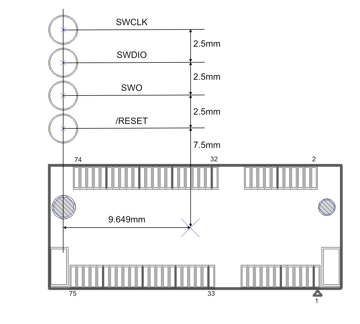
JTAG and SWD
The B523 module has 4 pads at the bottom exposing the SWD interface of the nRF52840. This interface can be used to debug your code or reprogram your B523 bootloader, device OS, or the user firmware. We use 4 pogo-pins connecting to these pads during production for firmware flashing.
Memory map
nRF52840 flash layout overview
- Bootloader (48KB, @0xF4000)
- User Application
- 256KB @ 0xB4000 (Device OS 3.1 and later)
- 128KB @ 0xD4000 (Device OS 3.0 and earlier)
- System (656KB, @0x30000)
- SoftDevice (192KB)
External SPI flash layout overview (dfu offset: 0x80000000)
- Reserved (4MB, @0x0040000)
- OTA (1500KB, @0x00289000)
- Reserved (420KB, @0x00220000)
- FAC (128KB, @0x00200000)
- LittleFS (2M, @0x00000000)
Pins and button definitions
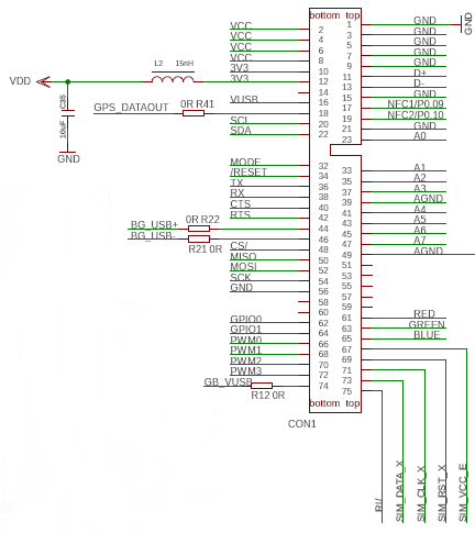
Pinout diagram

Common SoM pins
RESERVED and SOM pins may vary across different SoM models. If you are designing for this specific module, or similar modules, you can use the indicated functions even if the pin is marked RESERVED. Most nRF52840-based modules will have the same pin functions on the RESERVED pins.
The nRF52840 B-SoM has some differences from the RTL8722 M-SoM. Future modules with a different MCU may have different pin functions. An effort will be made to assign all of the listed functions for ADC, PWM, SPI, etc. from the set of common SoM pin functions in future modules, but the functions on RESERVED and SOM pins will likely vary.
Pin description
| # | Pin | Common | Function | nRF52 | Description |
|---|---|---|---|---|---|
| 1 | GND | GND | POWER | System ground. | |
| 2 | VCC | VCC5 | POWER | System power in, connect to the +LiPo or supply a fixed 3.6-4.3v power. | |
| 3 | GND | GND | POWER | System ground. | |
| 4 | VCC | VCC | POWER | System power in, connect to the +LiPo or supply a fixed 3.6-4.3v power. | |
| 5 | GND | GND | POWER | System ground. | |
| 6 | VCC | VCC | POWER | System power in, connect to the +LiPo or supply a fixed 3.6-4.3v power. | |
| 7 | GND | GND | POWER | System ground. | |
| 8 | VCC | VCC | POWER | System power in, connect to the +LiPo or supply a fixed 3.6-4.3v power. | |
| 9 | GND | GND | POWER | System ground. | |
| 10 | 3V3 | 3V3 | POWER | System power in, supply a fixed 3.0-3.6v power. | |
| 11 | USB D+ | USB D+ | IO | Data+ pin of the NRF52840 USB port. | |
| 12 | 3V3 | 3V3 | POWER | System power in, supply a fixed 3.0-3.6v power. | |
| 13 | USB D- | USB D- | IO | Data- pin of the NRF52840 USB port. | |
| 14 | NC | RESERVED3 | NC | Leave unconnected. | |
| 15 | GND | GND | POWER | System ground. | |
| 16 | VUSB | VUSB | POWER | System power in, USB detect pin for nRF52840. 5V on this pin enables the USB interface. | |
| 17 | NFC1 | SOM33 | NFC input | P0.09 | NFC antenna connection. |
| 18 | NC | RESERVED3 | NC | Leave unconnected. | |
| 19 | NFC2 | SOM43 | NFC input | P0.10 | NFC antenna connection. |
| 20 | D1 | SCL | IO | P0.27 | I2C SCL, and digital only GPIO. |
| 21 | GND | GND | POWER | System ground. | |
| 22 | D0 | SDA | IO | P0.26 | I2C SDA, and digital only GPIO. |
| 23 | A0 | ADC0 | IO | P0.03 | Analog input ADC02, and digital GPIO. |
| 32 | MODE | MODE | IO | P0.25 | Connected to the MODE button input, and digital only GPIO. |
| 33 | A1 | ADC1 | IO | P0.04 | Analog input ADC12, and digital GPIO. |
| 34 | RESET | RESET | I | Active-low reset input. | |
| 35 | A2 | ADC2 | IO | P0.28 | Analog input ADC22, and digital GPIO. |
| 36 | D9 | TX | IO | P0.06 | Primarily used as UART TX, but can also be used as a digital GPIO. |
| 37 | A3 | ADC3 | IO | P0.29 | Analog input ADC32, and digital GPIO. |
| 38 | D10 | RX | IO | P0.08 | Primarily used as UART RX, but can also be used as a digital GPIO. |
| 39 | AGND | AGND | POWER | System analog ground. | |
| 40 | D3 | RESERVED3 | IO | P1.10 | UART flow control CTS, SCL1 (Wire1), SPI1 MOSI, digital only GPIO. |
| 41 | A4 | RESERVED3 | IO | P0.30 | Analog input ADC42, and digital GPIO. |
| 42 | D2 | RESERVED3 | IO | P1.02 | UART flow control RTS, SDA1 (Wire1), SPI1 SCK, digital only GPIO. |
| 43 | A5 | RESERVED3 | IO | P0.31 | Analog input ADC52, and digital GPIO. |
| 44 | Quectel USB D+ | SOM0 | IO | Data+ pin of the cellular modem USB port. | |
| 45 | A6 | RESERVED3 | IO | P0.05 | Analog input ADC62, and digital GPIO. |
| 46 | Quectel USB D- | SOM1 | IO | Data- pin of the cellular modem USB port. | |
| 47 | A7 | RESERVED3 | IO | P0.02 | Analog input ADC72, and digital GPIO. |
| 48 | D8 | CS | IO | P0.07 | SPI interface CS, and digital only GPIO. |
| 49 | AGND | AGND | POWER | System analog ground. | |
| 50 | D11 | MISO | IO | P1.08 | SPI interface MISO, and digital only GPIO. |
| 51 | NC | RESERVED3 | NC | Leave unconnected. | |
| 52 | D12 | MOSI | IO | P1.09 | SPI interface MOSI, and digital only GPIO. |
| 53 | NC | RESERVED3 | NC | Leave unconnected. | |
| 54 | D13 | SCK | IO | P0.11 | SPI interface SCK, and digital only GPIO. |
| 55 | NC | RESERVED3 | NC | Leave unconnected. | |
| 56 | GND | GND | POWER | System analog ground. | |
| 57 | NC | RESERVED3 | NC | Leave unconnected. | |
| 58 | NC | RESERVED3 | NC | Leave unconnected. | |
| 59 | NC | RESERVED3 | NC | Leave unconnected. | |
| 60 | NC | RESERVED3 | NC | Leave unconnected. | |
| 61 | RGBR | RED | IO | P0.16 | Red pin of the RGB LED. |
| 62 | D22 | GPIO0 | IO | P1.01 | GPIO0, digital only. |
| 63 | RGBG | GREEN | IO | P0.15 | Green pin of the RGB LED. |
| 64 | D23 | GPIO1 | IO | P1.03 | GPIO1, digital only. |
| 65 | RGBB | BLUE | IO | P0.14 | Blue pin of the RGB LED. |
| 66 | D4 | PWM0 | IO | P0.12 | SPI1 MISO, Digital only GPIO, and PWM0. |
| 67 | SIM_VCC1 | SOM53 | POWER | Leave unconnected, 1.8V/3V SIM Supply Output from cellular modem. | |
| 68 | D5 | PWM1 | IO | P0.24 | Digital only GPIO, and PWM1. |
| 69 | SIM_RST1 | SOM63 | IO | Leave unconnected, 1.8V/3V SIM Reset Output from cellular modem. | |
| 70 | D6 | PWM2 | IO | P1.04 | Digital only GPIO, and PWM2. |
| 71 | SIM_CLK1 | SOM73 | IO | Leave unconnected, 1.8V/3V SIM Clock Output from cellular modem. | |
| 72 | D7 | PWM3 | IO | P0.13 | Digital only GPIO, and PWM3. |
| 73 | SIM_DATA1 | SOM83 | IO | Leave unconnected, 1.8V/3V SIM Data I/O of cellular modem with internal 4.7 k pull-up. | |
| 74 | Quectel VBUS | SOM23 | IO | USB detect pin for cellular modem. 5V on this pin enables the Quectel USB interface. | |
| 75 | Quectel RI | SOM94 | IO | Ring indicator |
1These pins are connected to the internal MFF2 SIM and should be left open.
2A0-A7 are 12-bit Analog-to-Digital (A/D) inputs (0-4095).
3SoM-specific and Reserved pins will vary depending on module. They are able to be used on the B523, but their function may be be different on future modules.
4RI is available on the B523 (Quectel) but not on the B402 (u-blox LTE M1)
5The VCC maximum is 4.3V on the B523 (Quectel) but is 4.2V on the B402 (u-blox LTE M1). For compatibility across modules, limit this to 4.2V.
By default, the Tinker application firmware enables the use of the bq24195 PMIC and MAX17043 fuel gauge. This in turn uses I2C (D0 and D1) and pin A6 (PM_INT). If you are not using the PMIC and fuel gauge and with to use these pins for other purposes, be sure to disable system power configuration. This setting is persistent, so you may want to disable it with your manufacturing firmware only.
System.setPowerConfiguration(SystemPowerConfiguration());
If you are using Ethernet with the B-Series SoM, the following pins are used by Ethernet:
| Device OS Pin | M.2 Pin | Ethernet Pin |
|---|---|---|
| MISO | 50 | SPI MISO |
| MOSI | 52 | SPI MOSI |
| SCK | 54 | SPI SCK |
| A7 | 47 | nRESET |
| D22 | 62 | nINTERRUPT |
| D8 | 48 | nCHIP SELECT |
Cellular modem USB pins
The cellular modem USB pins are optional on custom base boards. These pins are used for low-level diagnostics and reprogramming the cellular modem firmware.
Note, however, the Particle has never done a cellular modem firmware upgrade in the field because doing so generally requires recertification, and is there is a high likelihood that the upgrade will fail, rendering the modem unusable.
Cellular modem could be reprogrammed by removing the SoM from your board and putting it in the M.2 SoM breakout board, which has the cellular modem USB connector.
| # | Pin | Common | Function | nRF52 | Description |
|---|---|---|---|---|---|
| 44 | Quectel USB D+ | SOM0 | IO | Data+ pin of the cellular modem USB port. | |
| 46 | Quectel USB D- | SOM1 | IO | Data- pin of the cellular modem USB port. | |
| 74 | Quectel VBUS | SOM23 | IO | USB detect pin for cellular modem. 5V on this pin enables the Quectel USB interface. | |
| 75 | Quectel RI | SOM94 | IO | Ring indicator |
Complete module pin details


LED status
System RGB LED
Unlike the Boron, the B523 module does not have an on-module RGB system status LED. We have provided its individual control pins for you to connect an LED of your liking. This will allow greater flexibility in the end design of your products.
A detailed explanation of different color codes of the RGB system LED can be found here.
PMIC Notes
When using the B-Series SoM with a bq24195 PMIC, note the following:
By default, the bq24195 sets the input current limit, which affects powering by VIN and VUSB, to 100 mA. This affects the VSYS output of the PMIC, which powers both the cellular modem and 3V3 supply, and is not enough to power the B-Series SoM in normal operation.
If your device has the default firmware (Tinker), it will attempt to connect to the cloud, brown out due to insufficient current, then the device will reset. This may result in what appears to be the status LED blinking white, but is actually rolling reboot caused by brownout.
A factory new B-Series SoM does not enable the PMIC setup. To enable the use of the bq21415, you must enable the system power feature PMIC_DETECTION in your code. This defaults to off because the B-Series SoM can be used without a PMIC, or with a different PMIC, and also requires I2C on D0/D1, and some base boards may use those pins as GPIO.
Because the input current limit does not affect the battery input (Li+), for troubleshooting purposes it can be helpful to attach a battery to help rule out input current limit issues. It's also possible to supply 3.7V via a bench power supply to the battery input, instead of VIN.
The input current limit can result in a situation where you can't bring up a B-Series SoM because it browns out continuously, but also cannot flash code to it to stop if from browning out. There are two general solutions:
- Attach a battery or supply by Li+ when bringing up a board.
- Use SWD/JTAG and reset halt the MCU. This will prevent it from connecting to the cloud, so you can flash Device OS and firmware to it by SWD.
The input current limit is actually controlled by three factors:
- The power source max current setting in the PMIC. The default is 900 mA. It can be set to 100, 150, 500, 900, 1200, 1500, 2000, or 3000 mA.
- It is also limited by the hardware ILIM resistor. On Particle devices with a built-in PMIC, this is set to 1590 mA, but if you are implementing your own PMIC hardware, you can adjust this higher.
- When connected by USB, it will use DPDM, current negotiation via the USB DP (D+) and DM (D-) lines.
Note that some 2A tablet chargers and multi-port USB power supplies supply 2A but do not implement DPDM; these will be treated as if VIN was used, and you must set the power source current, otherwise the input current will be limited to 900 mA, which is not enough to power a 2G/3G cellular modem without an attached battery.
Technical specifications
Absolute maximum ratings [1]
Supply voltages
| Parameter | Symbol | Min | Typ | Max | Unit |
|---|---|---|---|---|---|
| Supply voltages | |||||
| Supply Input Voltage | VCC | -0.3 | +4.7 | V | |
| Supply Input Voltage | 3V3 | -0.3 | +3.9 | V | |
| VBUS USB supply voltage | VUSB | -0.3 | +5.8 | V | |
| I/O pin voltage | |||||
| VI/O, VDD ≤ 3.6 V | IO | -0.3 | VDD + 0.3 | V | |
| VI/O, VDD > 3.6 V | IO | -0.3 | +3.9 | V | |
| NFC antenna pin current | |||||
| INFC1/2 | NFC1/NFC2 | 80 | mA | ||
| Radio | |||||
| BT RF input level (52840) | 10 | dBm | |||
| Environmental | |||||
| Storage temperature | -40 | +85 | °C |
[1] Stresses beyond those listed under absolute maximum ratings may cause permanent damage to the device. These are stress ratings only, and functional operation of the device at these or any other conditions beyond those indicated under recommended operating conditions is not implied. Exposure to absolute-maximum-rated conditions for extended periods may affect device reliability.
Recommended operating conditions
| Parameter | Symbol | Min | Typ | Max | Unit |
|---|---|---|---|---|---|
| Supply voltages | |||||
| Supply Input Voltage | VCC | +3.6 | +3.8 | +4.3 | V |
| Supply Input Voltage | 3V3 | +3.0 | +3.3 | +3.6 | V |
| VBUS USB supply voltage | VUSB | +4.35 | +5.0 | +5.5 | V |
| Environmental | |||||
| Normal operating temperature1 | -20 | +25 | +753 | °C | |
| Extended operating temperature2 | -40 | +85 | °C | ||
| Humidity Range Non condensing, relative humidity | 95 | % |
Notes:
1 Normal operating temperature range (fully functional and meet 3GPP specifications).
2 Extended operating temperature range (RF performance may be affected outside normal operating range, though module is fully functional)
3 The maximum operating temperature is 75°C on the B523 (Quectel) but is 65°C on the B402 (u-blox LTE M1). For compatibility across modules, limit this to 65°C.
Power consumption
| Parameter | Symbol | Min | Typ | Peak | Unit |
|---|---|---|---|---|---|
| Operating Current (uC on, peripherals and radio disabled) | Iidle | 4.47 | 4.48 | 4.51 | mA |
| Operating Current (uC on, cellular on but not connected) | Icell_idle | 17.5 | 34.2 | 744 | mA |
| Operating Current (uC on, cellular connecting to tower) | Icell_conn_twr | 17.9 | 72.3 | 711 | mA |
| Operating Current (uC on, cellular connecting to cloud) | Icell_conn_cloud | 23.0 | 93.6 | 669 | mA |
| Operating Current (uC on, cellular connected but idle) | Icell_cloud_idle | 22.9 | 26.8 | 149 | mA |
| Operating Current (uC on, cellular connected and transmitting) | Icell_cloud_tx | 113 | 139 | 519 | mA |
| STOP mode sleep, GPIO wake-up | Istop_gpio | 323 | 538 | 916 | uA |
| STOP mode sleep, analog wake-up | Istop_analog | 272 | 537 | 948 | uA |
| STOP mode sleep, RTC wake-up | Istop_intrtc | 264 | 537 | 947 | uA |
| STOP mode sleep, BLE wake-up, advertising | Istop_ble_adv | 604 | 2260 | uA | |
| STOP mode sleep, BLE wake-up, connected | Istop_ble_conn | 619 | 1700 | uA | |
| STOP mode sleep, serial wake-up | Istop_usart | 327 | 537 | 912 | uA |
| STOP mode sleep, cellular wake-up | Istop_cell | 18.7 | 23.1 | 140 | mA |
| ULP mode sleep, GPIO wake-up | Iulp_gpio | 53.6 | 446 | uA | |
| ULP mode sleep, analog wake-up | Iulp_analog | 55.8 | 420 | uA | |
| ULP mode sleep, RTC wake-up | Iulp_intrtc | 54.8 | 444 | uA | |
| ULP mode sleep, BLE wake-up, advertising | Iulp_ble_adv | 139 | 2430 | uA | |
| ULP mode sleep, BLE wake-up, connected | Iulp_ble_conn | 162 | 1090 | uA | |
| ULP mode sleep, serial wake-up | Iulp_usart | 317 | 537 | 938 | uA |
| ULP mode sleep, cellular wake-up | Iulp_cell | 18.4 | 22.8 | 149 | mA |
| HIBERNATE mode sleep, GPIO wake-up | Ihib_gpio | 29.7 | 430 | uA | |
| HIBERNATE mode sleep, analog wake-up | Ihib_analog | 30.8 | 441 | uA |
1The min, and particularly peak, values may consist of very short transients. The typical (typ) values are the best indicator of overall power consumption over time. The peak values indicate the absolute minimum capacity of the power supply necessary, not overall consumption.
Current measurements taken at 3.6V via the battery input. For more information about measuring power usage, see power measurement.
Radio specifications
Boron has two radio modules.
nRF52840
- Bluetooth® 5, 2.4 GHz
- 95 dBm sensitivity in 1 Mbps Bluetooth® low energy mode
- 103 dBm sensitivity in 125 kbps Bluetooth® low energy mode (long range)
- 20 to +8 dBm TX power, configurable in 4 dB steps
4G LTE cellular characteristics for EG91-E
| Parameter | Value |
|---|---|
| Protocol stack | 3GPP Release 13 |
| RAT | LTE Cat 1 |
| LTE FDD Bands | Band 28A (700 MHz) |
| Band 20 (800 MHz) | |
| Band 8 (900 MHz) | |
| Band 3 (1800 MHz) | |
| Band 1 (2100 MHz) | |
| Band 7 (2600 MHz) | |
| WCDMA Bands | Band 8 (900 MHz) |
| Band 1 (2100) | |
| GSM Bands | EGSM900 (900 MHz) |
| DCS1800 (1800 MHz) | |
| Power class | Class 4 (33dBm ± 2dB) for EGSM900 |
| Class 1 (30dBm ± 2dB) for DCS1800 | |
| Class E2 (27dBm ± 3dB) for EGSM900 8-PSK | |
| Class E2 (26dBm ± 3dB) for DCS1800 8-PSK | |
| Class 3 (24dBm ± 3dB) for WCDMA bands | |
| Class 3 (23dBm ± 2dB) for LTE FDD bands |
I/O characteristics
These specifications are based on the nRF52840 datasheet.
| Symbol | Parameter | Min | Typ | Max | Unit |
|---|---|---|---|---|---|
| VIH | Input high voltage | 0.7 xVDD | VDD | V | |
| VIL | Input low voltage | VSS | 0.3 xVDD | V | |
| VOH,SD | Output high voltage, standard drive, 0.5 mA, VDD ≥1.7 | VDD - 0.4 | VDD | V | |
| VOH,HDH | Output high voltage, high drive, 5 mA, VDD >= 2.7 V | VDD - 0.4 | VDD | V | |
| VOH,HDL | Output high voltage, high drive, 3 mA, VDD >= 1.7 V | VDD - 0.4 | VDD | V | |
| VOL,SD | Output low voltage, standard drive, 0.5 mA, VDD ≥1.7 | VSS | VSS + 0.4 | V | |
| VOL,HDH | Output low voltage, high drive, 5 mA, VDD >= 2.7 V | VSS | VSS + 0.4 | V | |
| VOL,HDL | Output low voltage, high drive,3 mA, VDD >= 1.7 V | VSS | VSS + 0.4 | V | |
| IOL,SD | Current at VSS+0.4 V, output set low, standard drive, VDD≥1.7 | 1 | 2 | 4 | mA |
| IOL,HDH | Current at VSS+0.4 V, output set low, high drive, VDD >= 2.7V | 6 | 10 | 15 | mA |
| IOL,HDL | Current at VSS+0.4 V, output set low, high drive, VDD >= 1.7V | 3 | mA | ||
| IOH,SD | Current at VDD-0.4 V, output set high, standard drive, VDD≥1.7 | 1 | 2 | 4 | mA |
| IOH,HDH | Current at VDD-0.4 V, output set high, high drive, VDD >= 2.7V | 6 | 9 | 14 | mA |
| IOH,HDL | Current at VDD-0.4 V, output set high, high drive, VDD >= 1.7V | 3 | mA | ||
| tRF,15pF | Rise/fall time, standard drivemode, 10-90%, 15 pF load1 | 9 | ns | ||
| tRF,25pF | Rise/fall time, standard drive mode, 10-90%, 25 pF load1 | 13 | ns | ||
| tRF,50pF | Rise/fall time, standard drive mode, 10-90%, 50 pF load1 | 25 | ns | ||
| tHRF,15pF | Rise/Fall time, high drive mode, 10-90%, 15 pF load1 | 4 | ns | ||
| tHRF,25pF | Rise/Fall time, high drive mode, 10-90%, 25 pF load1 | 5 | ns | ||
| tHRF,50pF | Rise/Fall time, high drive mode, 10-90%, 50 pF load1 | 8 | ns | ||
| RPU | Pull-up resistance | 11 | 13 | 16 | kΩ |
| RPD | Pull-down resistance | 11 | 13 | 16 | kΩ |
| CPAD | Pad capacitance | 3 | pF | ||
| CPAD_NFC | Pad capacitance on NFC pads | 4 | pF | ||
| INFC_LEAK | Leakage current between NFC pads when driven to different states | 1 | 10 | μA |
Rise and fall times based on simulations
GPIO default to standard drive (2mA) but can be reconfigured to high drive (9mA) in Device OS 2.0.0 and later using the
pinSetDriveStrength()function.
Mechanical specifications
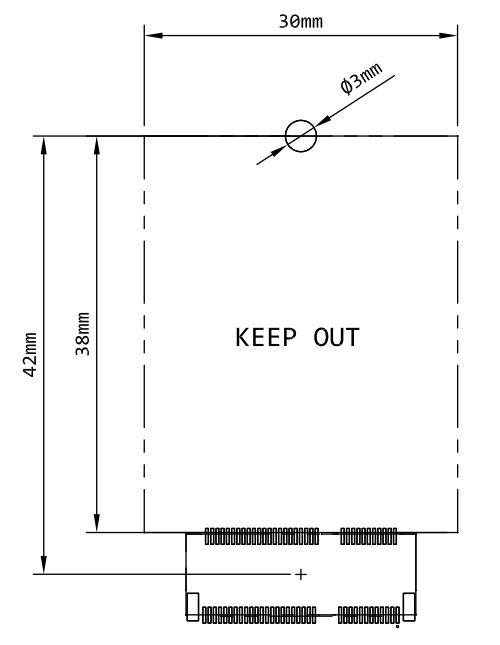
Dimensions and weight
| Parameters | Value | Unit |
|---|---|---|
| Width | 30 | mm |
| Height | 42 | mm |
| Thickness | 5.5 | mm |
| Weight | 6.2 | grams |
Mechanical drawing
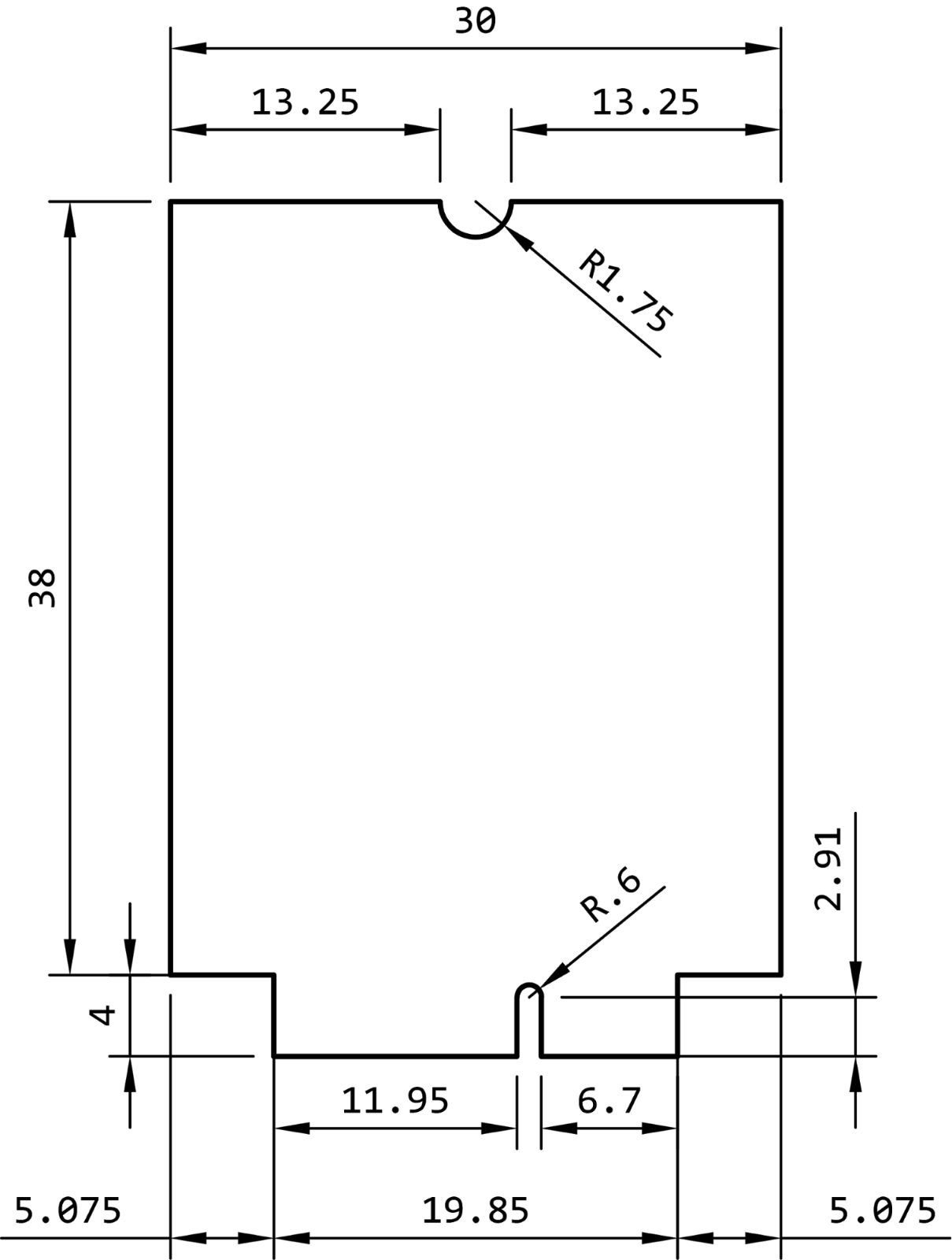
Dimensions are in millimeters.
3D models
3D models of the B-Series SoM module are available in the hardware-libraries Github in formats including step, iges, stl, and f3d.
The 3D models are the same for the B524 and B523, as the only changes are the SIM card, which is not visible.
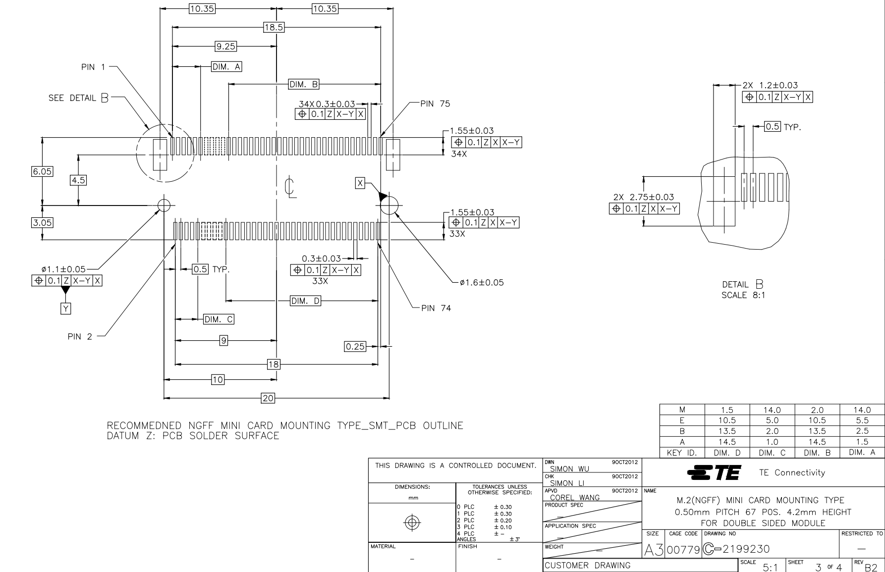
Mating connector and land pattern
The mating connector is a an M.2 (NGFF) type 4. Note that there are several different key configurations for the M.2, and type 4 is different than is commonly used on SSDs.
One compatible connector is the TE 2199230-4. It is widely available including at suppliers such as DigiKey.
Screw assembly
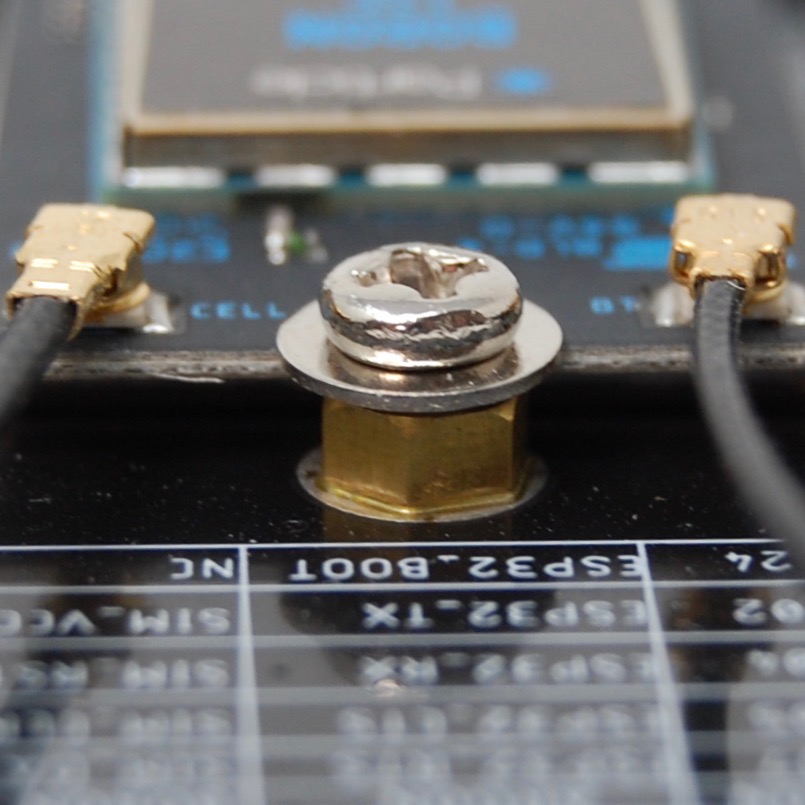
We recommend this screw assembly to securely affix the B series SoM to your circuit board. From top to bottom:
- M3 screw, 3mm long
- M3 washer
- M3 standoff, 2.45mm
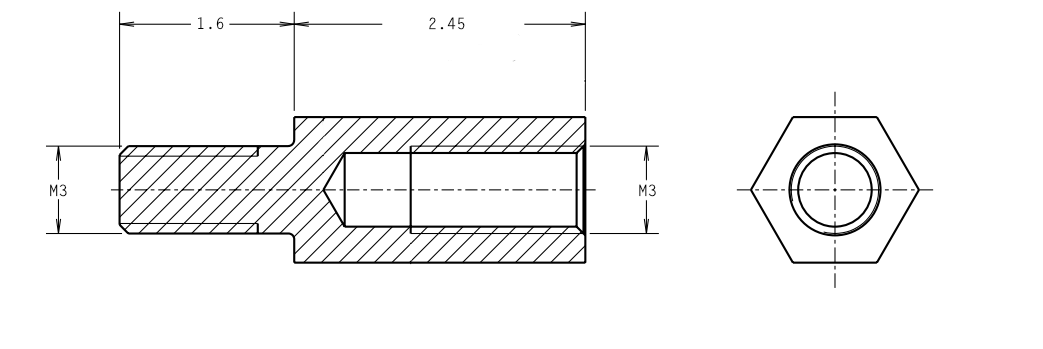
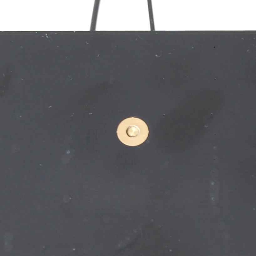
- Mounting hole, 2.6 mm metal hole, 3.1mm metal ring diameter (picture is of the bottom side of the circuit board)
An alternative design uses a JAE SM3ZS067U410-NUT1-R1200 standoff. It's reflow soldered to your base board and has a threaded hole for a M2*3 screw to hold down the SoM. This may be easier to obtain.
Note that a hold-down screw is required because the M.2 connector does not have integrated locks and the SoM will pop up if not attached to the base board.
The screw should be connected to the ground plane on your base board.
Design considerations
We strongly recommend against placing components under the SOM board because there is not enough height.
Product handling
ESD precautions
The B series contains highly sensitive electronic circuitry and is an Electrostatic Sensitive Device (ESD). Handling an B series without proper ESD protection may destroy or damage it permanently. Proper ESD handling and packaging procedures must be applied throughout the processing, handling and operation of any application that incorporates the B series module. ESD precautions should be implemented on the application board where the B series is mounted. Failure to observe these precautions can result in severe damage to the B series!
Connectors
The U.FL antenna connector is not designed to be constantly plugged and unplugged. The antenna pin is static sensitive and you can destroy the radio with improper handling. A tiny dab of glue (epoxy, rubber cement, liquid tape or hot glue) on the connector can be used securely hold the plug in place.
The M.2 edge connector is static sensitive and should be handled carefully. The M.2 connector is not designed for repeated removal and insertion of the module.
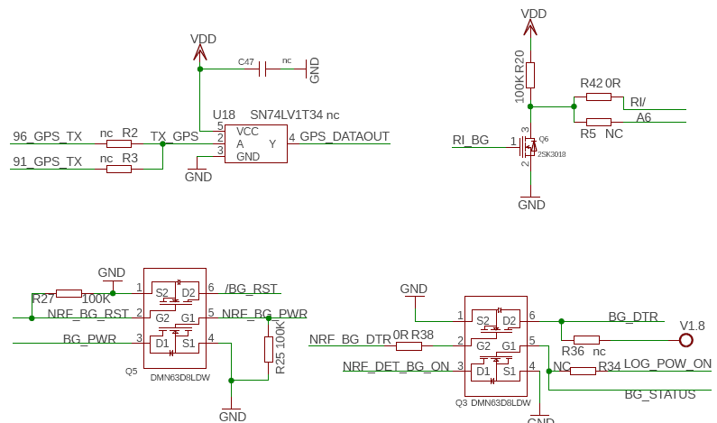
Schematics
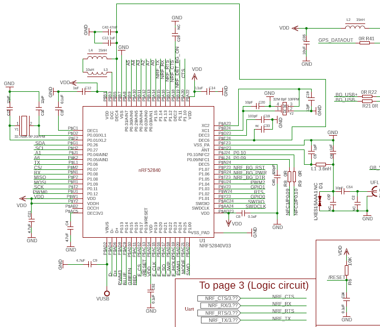
Microcontroller
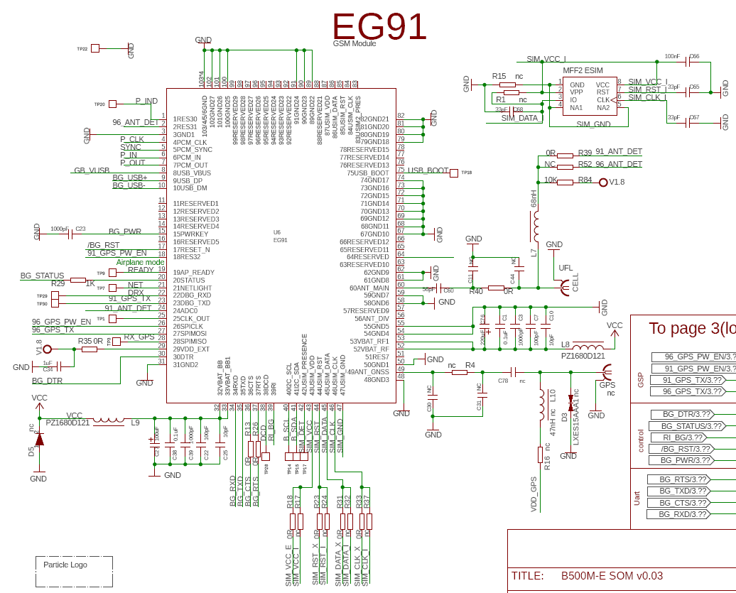
Quectel cellular modem
M.2 connector
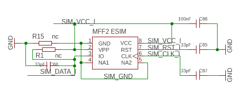
SIM and Flash
Buffers
Assembly
Conformal coatings
B-Series SoM modules should not use a conformal coating to protect the module from water. Some components on the SoM cannot be coated and would need to be masked off during coating. This will make the coating process difficult to implement and test.
Furthermore, you cannot safely protect the the connection between the M.2 SoM and the M.2 NGFF connector by using a coating. Using an enclosure that protects both your base board and the B-Series SoM as a single waterproof assembly is recommended instead.
Default settings
The B series comes pre-programmed with a bootloader and a user application called Tinker. This application works with an iOS and Android app also named Tinker that allows you to very easily toggle digital pins, take analog and digital readings and drive variable PWM outputs.
The bootloader allows you to easily update the user application via several different methods, USB, OTA, Serial Y-Modem, and also internally via the Factory Reset procedure. All of these methods have multiple tools associated with them as well.
Certification
EU declaration of conformity
We, Particle Industries, Inc., declare under our sole responsibility that the product, B524 and B523, to which this declaration relates, is in conformity with RED Directive 2014/53/EU and (EU) 2015/863 RoHS Directive 2011/65/EU (Recast).
The full text of the EU declaration of conformity is available at the following Internet address https://www.particle.io/.
Radiation Exposure Statement: This equipment complies with radiation exposure limits set forth for an uncontrolled environment.
The operating frequency bands and the maximum transmitted power limit are listed below:
- BLE 2402-2480MHz, 10dBm
- LTE (CAT-1 bands B1 B3 B7 B8 B20 B28), Frequency Ranges: 703-960MHz, 1710-2170MHz, 2550-2690MHz, Max TX Power: 25dBm
- 3G (WCDMA sits on LTE B1, B8), Frequency Ranges: 880-960MHz, 1920-2170 MHz, Max TX Power: 25dBm
- 2G (EGSM900 sits on LTE B8), Frequency Ranges: 880-915MHz, 925-960 MHz, Max TX Power: 35dBm
- 2G (DCS1800 sits on LTE B3), Frequency Ranges: 1710.2-1784.8MHz, 1805.2-1879.8MHz, Max TX Power: 32dBm
United Kingdom
UKCA Conformity:
Radio Equipment Regulations 2017 (S.I. 2017/1206)
Certification documents
CE (Europe) - B523 B524 B-Series SoM
- Summary (updated 2021-09-16)
- EMC Test Report (updated 2021-09-16)
- RED BLE Test Report (updated 2022-11-09)
- RED Cellular Test Report (updated 2021-09-16)
- EN 300 328 Test Report (2.4 GHz ISM band) (updated 2022-11-09)
- EN 300 330 Test Report (NFC) (updated 2022-11-09)
- EN 301 489 Test Report (updated 2022-11-09)
- EN 301 511 Test Report (GSM) (updated 2022-11-09)
- EN 301 908 Variant Radio Test Report (updated 2022-11-09)
- EN-62311 Test Report (updated 2022-11-09)
- EN-62368 Test Report (supersedes EN-60950) (updated 2022-11-09)
- RoHS 3.0 Test Report (updated 2021-09-16)
FCC (United States) - B523 B524 B-Series SoM
The B523 and B524 are not FCC certified as it does not support any cellular bands used in the United States. The B404X should be used instead.
ISED (Canada) - B523 B524 B-Series SoM
The B523 and B524 are not ISED certified as it does not support any cellular bands used in the Canada. The B404X should be used instead.
RoHS - B523 B524 B-Series SoM
UKCA (United Kingdom) - B523 B524 B-Series SoM
- UKCA Certification (updated 2022-11-09)
Japan - B524 B-Series SoM
Country compatibility
| Country | Model | Technologies | Carriers |
|---|---|---|---|
| Albania | B524 | 2G, 3G, 4G | Eagle, Telekom, Vodafone |
| Algeria | B524 | 2G, 3G, 4G | Mobilis, Ooredoo |
| Aruba | B524 | 2G, 3G, 4G | Setar |
| Australia | B524 | 4G | Optus, Telstra, Vodafone |
| Austria | B524 | 2G, 4G | 3 (Drei), A1, T-Mobile |
| Bahrain | B524 | 2G, 4G | Zain |
| Bangladesh | B524 | 2G, 3G, 4G | Bangalink, GrameenPhone |
| Belarus | B524 | 2G, 3G, 4G | A1 |
| Belgium | B524 | 2G, 4G | Base, Orange, Proximus |
| Bosnia and Herzegovina | B524 | 2G, 3G | HT Eronet |
| Botswana | B524 | 2G, 3G, 4G | BeMobile |
| Brunei | B524 | 3G, 4G | DST |
| Bulgaria | B524 | 2G, 3G | A1, Telenor, Vivacom |
| Burkina Faso | B524 | 2G, 3G, 4G | Orange |
| Cabo Verde | B524 | 2G, 3G, 4G | CVMóvel, Unitel T+ |
| Cambodia | B524 | 2G, 3G | Metfone |
| Chad | B524 | 2G, 3G, 4G | Airtel |
| Chile | B524 | 3G, 4G | Claro, Entel, Movistar |
| Congo (Brazzaville) | B524 | 2G, 3G, 4G | Airtel |
| Congo (Kinshasa) | B524 | 2G, 3G, 4G | Airtel |
| Côte d'Ivoire | B524 | 2G, 3G | MTN |
| Croatia | B524 | 2G, 3G, 4G | Hrvatski Telekom, Tele2 |
| Cyprus | B524 | 2G, 3G, 4G | MTN, PrimeTel |
| Czechia | B524 | 2G, 4G | O2, T-Mobile, Vodafone |
| Denmark | B524 | 2G, 4G | 3 (Tre), TDC, Telenor, Telia |
| Egypt | B524 | 2G, 3G, 4G | Etisalat, Orange |
| Estonia | B524 | 2G, 3G, 4G | Elisa, Tele2, Telia |
| eSwatini | B524 | 2G, 3G, 4G | MTN |
| Ethiopia | B524 | 2G, 3G, 4G | Ethio Telecom |
| Faroe Islands | B524 | 2G, 3G | Faroese Telecom, Vodafone |
| Finland | B524 | 2G, 4G | DNA, Elisa, Telia |
| France | B524 | 2G, 3G, 4G | Bouygues, Free Mobile, Orange, SFR |
| French Guiana | B524 | 2G, 3G | Digicel |
| Gabon | B524 | 2G, 3G, 4G | Airtel |
| Germany | B524 | 2G, 3G, 4G | O2, Telekom, Vodafone |
| Ghana | B524 | 2G, 3G, 4G | AirtelTigo, MTN, Vodafone |
| Gibraltar | B524 | 2G, 3G, 4G | Gibtel |
| Greece | B524 | 2G, 4G | Cosmote, Vodafone, Wind |
| Guadeloupe | B524 | 2G, 3G, 4G | Orange |
| Guinea | B524 | 2G, 3G, 4G | MTN |
| Guinea-Bissau | B524 | 2G, 3G, 4G | MTN |
| Guyana | B524 | 2G | Digicel |
| Haiti | B524 | 2G, 3G | Digicel |
| Hong Kong | B524 | 3G, 4G | CMHK, CSL, SmarTone |
| Hungary | B524 | 2G, 3G, 4G | Magyar Telekom, Telenor, Vodafone |
| Iceland | B524 | 4G | Nova, Siminn, Vodafone |
| Indonesia | B524 | 2G, 3G, 4G | Indosat, Telkomsel, XL Axiata |
| Ireland | B524 | 2G, 3G, 4G | 3 (Tre), Meteor, O2, Vodafone |
| Israel | B524 | 2G, 3G, 4G | Hot Mobile, Orange, Pelephone |
| Italy | B524 | 2G, 3G, 4G | TIM, Vodafone, Wind |
| Japan | B524 | 4G | KDDI, NTT DoCoMo, Softbank |
| Jordan | B524 | 2G, 3G, 4G | Zain |
| Kazakhstan | B524 | 2G, 3G, 4G | Beeline, K-Cell |
| Kenya | B524 | 2G, 3G, 4G | Airtel |
| Kuwait | B524 | 2G, 3G, 4G | Viva, Zain |
| Latvia | B524 | 2G, 4G | Bite, LMT, Tele2 |
| Liechtenstein | B524 | 2G, 3G, 4G | Mobilkom, Orange |
| Lithuania | B524 | 2G, 4G | Bite, Omnitel, Tele2 |
| Luxembourg | B524 | 2G, 4G | Orange, POST, Tango |
| Macao | B524 | 3G, 4G | CTM |
| Madagascar | B524 | 2G, 3G, 4G | Airtel |
| Malawi | B524 | 2G, 3G, 4G | Airtel |
| Malaysia | B524 | 2G, 3G, 4G | Celcom, DiGi, Maxis |
| Malta | B524 | 2G, 3G, 4G | Go Mobile, Vodafone |
| Moldova | B524 | 2G, 3G, 4G | Moldcell, Orange |
| Mongolia | B524 | 2G, 3G | Mobicom, Unitel |
| Montenegro | B524 | 2G, 3G, 4G | Mtel, T-Mobile, Telenor |
| Morocco | B524 | 2G, 3G, 4G | Inwi, Medi Telecom |
| Mozambique | B524 | 2G, 3G, 4G | Vodacom |
| Myanmar | B524 | 2G, 3G, 4G | MPT, Telenor |
| Namibia | B524 | 2G, 3G, 4G | Telecom Namibia |
| Netherlands | B524 | 2G, 3G, 4G | KPN, T-Mobile, Vodafone |
| New Zealand | B524 | 4G | 2degrees, Spark, Vodafone |
| Nigeria | B524 | 2G, 3G, 4G | 9mobile, Airtel, Glo, MTN |
| Norway | B524 | 2G, 3G, 4G | TDC, Telenor, Telia |
| Pakistan | B524 | 2G, 3G, 4G | Mobilink, Telenor, Ufone, Warid |
| Palestine | B524 | 2G, 3G | Jawwal |
| Papua New Guinea | B524 | 2G, 3G | bmobile |
| Poland | B524 | 2G, 3G, 4G | Orange, Play, Plus, T-Mobile |
| Portugal | B524 | 2G, 3G, 4G | NOS, TMN, Vodafone |
| Qatar | B524 | 2G, 3G, 4G | Ooredoo, Vodafone |
| Romania | B524 | 2G, 4G | Orange, Telekom Romania, Vodafone |
| Rwanda | B524 | 2G, 3G | Airtel, MTN |
| Serbia | B524 | 2G, 3G, 4G | Telenor, VIP |
| Seychelles | B524 | 2G, 3G, 4G | Airtel |
| Sint Maarten | B524 | 2G, 3G | TelCell |
| Slovakia | B524 | 2G, 4G | O2, Orange, Telekom |
| Slovenia | B524 | 2G, 3G, 4G | A1, Mobitel |
| South Africa | B524 | 2G, 3G, 4G | Cell C, MTN, Vodacom |
| South Korea | B524 | 3G, 4G | KT, LG U+, SK Telecom |
| South Sudan | B524 | 2G, 3G | MTN |
| Spain | B524 | 2G, 3G, 4G | Orange, Telefonica, Vodafone, Yoigo |
| Sri Lanka | B524 | 2G, 3G, 4G | Dialog, Mobitel |
| Suriname | B524 | 2G, 3G | Telesur |
| Sweden | B524 | 2G, 4G | 3 (Tre), Tele2, Telenor, Telia |
| Switzerland | B524 | 3G, 4G | Salt, Sunrise, Swisscom |
| Taiwan | B524 | 3G, 4G | Chunghwa, FarEasTone, T Star, Taiwan Mobile |
| Tanzania | B524 | 2G, 3G, 4G | Airtel |
| Thailand | B524 | 2G, 3G, 4G | AIS, DTAC, True Move |
| Tunisia | B524 | 2G, 3G, 4G | Orange Tunisie, Tunisie Telecom |
| Uganda | B524 | 2G, 3G, 4G | Africell, Airtel, MTN |
| United Kingdom | B524 | 2G, 4G | 3, EE, O2, Vodafone |
| Vietnam | B524 | 3G, 4G | MobiFone, Viettel, Vinaphone |
| Zambia | B524 | 2G, 3G, 4G | Airtel |
Ordering information
| SKU | Description | Region | Modem | EtherSIM | Lifecycle | Replacement |
|---|---|---|---|---|---|---|
| B524MEA | B-Series LTE CAT-1/3G/2G (Europe, EtherSIM) [x1] | EMEAA | EG91-E | ✓ | GA | |
| B524MTY | B-Series LTE CAT-1/3G/2G (Europe, EtherSIM), Tray [x50] | EMEAA | EG91-E | ✓ | GA | |
| B523MTY | B-Series LTE CAT-1/3G/2G (Europe), Tray [x50] | EMEAA | EG91-E | NRND | B524MTY | |
| B523MEA | B-Series LTE CAT-1/3G/2G (Europe) [x1] | EMEAA | EG91-E | Deprecated | B524MEA |
- EMEAA: Selected countries in Europe, Middle East, Africa, and Asia, including Australia and New Zealand. See the cellular carrier list for more information.
Revision history
| Revision | Date | Author | Comments |
|---|---|---|---|
| 001 | 27 Apr 2020 | RK | First Release |
| 002 | 30 Jul 2020 | RK | Added explanation of DIV connector |
| 003 | 16-Sep-2020 | RK | Added power consumption information |
| 004 | 04-Jan-2021 | RK | Fix incorrect pin number on pogo pin diagram |
| 005 | 15-Mar-2021 | RK | Updated model, carrier, ordering information |
| 006 | 23-Mar-2021 | RK | Pins 40 and 42 functions were reversed |
| 007 | 26-Apr-2021 | RK | Added B524 model number |
| 008 | 14-May-2021 | RK | Pins 40 and 42 were not actually reversed |
| 009 | 19-May-2021 | RK | List Ethernet reserved pins |
| 010 | 28-Jun-2021 | RK | Added Device OS 3.1 memory map information |
| 011 | 10-Sep-2021 | RK | Changed wording of peak vs. max current |
| 012 | 05-May-2022 | RK | Corrected number of PWM outputs (8) |
| 013 | 11-Aug-2022 | RK | Correct typo in 3V3 explanation |
| 014 | 29-Aug-2022 | RK | Added EU declaration of conformity |
| 015 | 16-Sep-2022 | RK | Added UKCA conformity |
| 016 | 31-Oct-2022 | RK | Updated EU operating frequencies |
| 017 | 10-Dec-2022 | RK | Added PMIC notes |
| 018 | 06-Jan-2022 | RK | Clarify power supply notes for VCC and 3V3 |
| 019 | 31-Jan-2023 | RK | Add Device OS versions |
| 020 | 28-Apr-2023 | RK | Add conformal coating warning |
| 021 | 13-Nov-2023 | RK | Add full pin details |
| 022 | 20-Dec-2023 | RK | Clarified band power information table |
| 023 | 20-Feb-2024 | RK | M.2 screw assembly should be connected to ground |
| 024 | 23-Apr-2024 | RK | Added links to certification documents |
| 025 | 2024-09-03 | RK | Added clarification of cellular modem USB pins |