
Photon Datasheet
Model number: PHOTONH, PHOTONNOH
The Photon has been deprecated. The recommended replacement is the Photon 2. See the Photon 2 Datasheet and Photon 2 from Photon migration guide for more information.
void setup() {
    Particle.publish("my-event","The internet just got smarter!");
}
Functional description
Overview
Particle's Internet of Things hardware development kit, the Photon, provides everything you need to build a connected product. Particle combines a powerful ARM Cortex M3 microcontroller with a Broadcom Wi-Fi chip in a tiny thumbnail-sized module called the PØ (P-zero).
To get you started quickly, Particle adds a rock solid 3.3VDC SMPS power supply, RF and user interface components to the PØ on a small single-sided PCB called the Photon. The design is open source, so when you're ready to integrate the Photon into your product, you can.
The Photon comes in two physical forms: with headers and without. Prototyping is easy with headers as the Photon plugs directly into standard breadboards and perfboards, and may also be mounted with 0.1" pitch female headers on a PCB. To minimize space required, the Photon form factor without headers has castellated edges. These make it possible to surface mount the Photon directly onto your PCB.
Features
- Particle PØ Wi-Fi module
- Broadcom BCM43362 Wi-Fi chip
- 802.11b/g/n Wi-Fi
- STM32F205RGY6 120Mhz ARM Cortex M3
- 1MB flash, 128KB RAM
- On-board RGB status LED (ext. drive provided)
- 18 Mixed-signal GPIO and advanced peripherals
- Open source design
- Real-time operating system (FreeRTOS)
- Soft AP setup
- FCC (United States), CE (European Union), and ISED (Canada) certified
Device OS Support
It is recommended that you use the latest version in the 2.x LTS release line with the all Photons.
While the devices are compatible with older versions of Device OS and 3.x, these versions as past the end-of-support date and are not recommended for use in production. Only 2.x LTS remains in the Extended Support and Maintenance (ESM) window.
For information on upgrading Device OS, see Version information. For the latest version shipped from the factory, see Manufacturing firmware versions page. See also Long Term Support (LTS) releases.
Interfaces
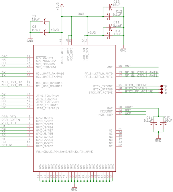
Block diagram
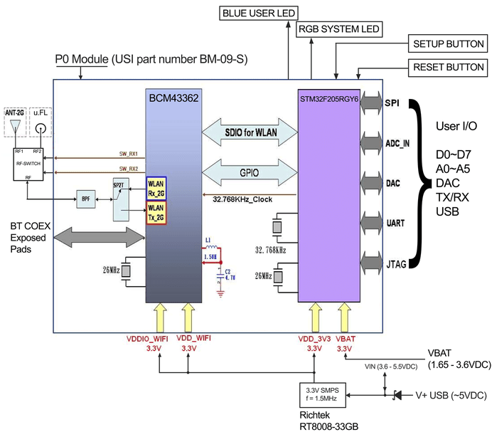
Power
Power to the Photon is supplied via the on-board USB Micro B connector or directly via the VIN pin. If power is supplied directly to the VIN pin, the voltage should be regulated between 3.6VDC and 5.5VDC. When the Photon is powered via the USB port, VIN will output a voltage of approximately 4.8VDC due to a reverse polarity protection series schottky diode between V+ of USB and VIN. When used as an output, the max load on VIN is 1A. 3V3 can also be used as an output, but has a limited overhead of only 100mA available. (Please refer to Absolute Maximum Ratings for more info).
Typical average current consumption is 80mA with 5V @ VIN with Wi-Fi on. Deep sleep quiescent current is typically 80uA (Please refer to Recommended Operating Conditions for more info). When powering the Photon from the USB connector, make sure to use a quality cable to minimize IR drops (current x resistance = voltage) in the wiring. If a high resistance cable (i.e., low current) is used, peak currents drawn from the Photon when transmitting and receiving will result in voltage sag at the input which may cause a system brown out or intermittent operation. Likewise, the power source should be sufficient enough to source 1A of current to provide an adequate amount of current overhead (especially if powering additional circuitry off of VIN).
Warning: When powering the Photon from long wires on USB and VIN, care should be taken to protect against damaging voltage transients. From the Richtek datasheet:
When a ceramic capacitor is used at the input and the power is supplied by a wall adapter through long wires, a load step at the output can induce ringing at the input, VIN. At best, this ringing can couple to the output and be mistaken as loop instability. At worst, a sudden inrush of current through the long wires can potentially cause a voltage spike at VIN large enough to damage the part.
To avoid these voltage spikes, keep input wiring as short as possible. If long wires are unavoidable, it is advisable to add a 5.1V zener diode or similar transient suppression device from VIN to GND. Another technique is adding more capacitance to the input using an electrolytic capacitor. Please refer to AN-88 by Linear for a good discussion on this topic.
RF
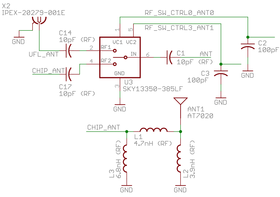
The RF section of the Photon is a finely tuned impedance controlled network of components that optimize the efficiency and sensitivity of the Wi-Fi communications.
An RF feed line runs from the PØ module into a SPDT RF-switch. Logic level control lines on the PØ module select which of the two ports of the RF-switch is connected to the RF feed line. A 100pF decoupling capacitor is located on each control line. One port is connected to a PCB ceramic chip antenna, and the other is connected to a U.FL connector for external antenna adaptation. The default port will be set to the chip antenna.
Additionally, a user API is available to switch between internal, external and even an automatic mode which continuously switches between each antenna and selects the best signal. All three RF ports on the RF-switch have a 10pF RF quality DC-blocking capacitor in series with them. These effectively pass 2.4GHz frequencies freely while blocking unwanted DC voltages from damaging the RF-switch. All RF traces are considered as tiny transmission lines that have a controlled 50 ohm impedance.
The chip antenna is impedance matched to the 50 ohm RF feed line via a Pi network comprised of three RF inductors (1 series, 2 shunt). These values are quite specific to the Photon due to the PCB construction and layout of the RF section. Even if the Photon's layout design is copied exactly, to achieve the best performance it would be worth re-examining the Pi network values on actual samples of the PCB in question.
FCC approved antennas
| Antenna Type | Manufacturer | MFG. Part # | Gain |
|---|---|---|---|
| Dipole antenna | LumenRadio | 104-1001 | 2.15dBi |
| Chip antenna | Advanced Ceramic X | AT7020-E3R0HBA | 1.3dBi |
Peripherals and GPIO
The Photon has ton of capability in a small footprint, with analog, digital and communication interfaces.
| Peripheral Type | Qty | Input(I) / Output(O) | FT[1] / 3V3[2] |
|---|---|---|---|
| Digital | 18 | I/O | FT/3V3 |
| Analog (ADC) | 8 | I | 3V3 |
| Analog (DAC) | 2 | O | 3V3 |
| SPI | 2 | I/O | 3V3 |
| I2S | 1 | I/O | 3V3 |
| I2C | 1 | I/O | FT |
| CAN | 1 | I/O | 3V3[4] |
| USB | 1 | I/O | 3V3 |
| PWM | 9[3] | O | 3V3 |
Notes:
[1] FT = 5.0V tolerant pins. All pins except A3 and DAC are 5V tolerant (when not in analog mode). If used as a 5V input the pull-up/pull-down resistor must be disabled.
[2] 3V3 = 3.3V max pins.
[3] PWM is available on D0, D1, D2, D3, A4, A5, WKP, RX, TX with a caveat: PWM timer peripheral is duplicated on two pins (A5/D2) and (A4/D3) for 7 total independent PWM outputs. For example: PWM may be used on A5 while D2 is used as a GPIO, or D2 as a PWM while A5 is used as an analog input. However A5 and D2 cannot be used as independently controlled PWM outputs at the same time.
[4] Technically these pins are 5.0V tolerant, but since you wouldn't operate them with a 5.0V transceiver it's proper to classify them as 3.3V.
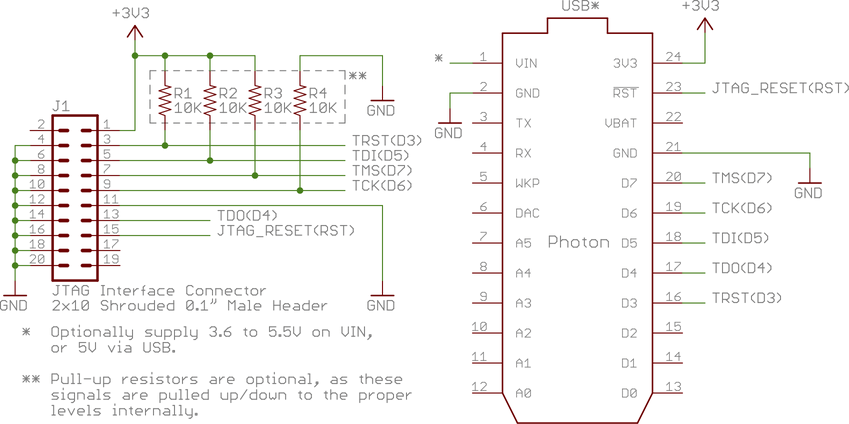
JTAG and SWD
Pin D3 through D7 are JTAG interface pins. These can be used to reprogram your Photon bootloader or user firmware image with standard JTAG tools such as the ST-Link v2, J-Link, R-Link, OLIMEX ARM-USB-TINI-H, and also the FTDI-based Particle JTAG Programmer. If you are short on available pins, you may also use SWD mode which requires less connections.
| Photon Pin | JTAG | SWD | STM32F205RGY6 Pin | PØ Pin # | PØ Pin Name | Default Internal[1] |
|---|---|---|---|---|---|---|
| D7 | JTAG_TMS | SWD/SWDIO | PA13 | 44 | MICRO_JTAG_TMS | ~40k pull-up |
| D6 | JTAG_TCK | CLK/SWCLK | PA14 | 40 | MICRO_JTAG_TCK | ~40k pull-down |
| D5 | JTAG_TDI | PA15 | 43 | MICRO_JTAG_TDI | ~40k pull-up | |
| D4 | JTAG_TDO | PB3 | 41 | MICRO_JTAG_TDO | Floating | |
| D3 | JTAG_TRST | PB4 | 42 | MICRO_JTAG_TRSTN | ~40k pull-up | |
| 3V3 | Power | Power | ||||
| GND | Ground | Ground | ||||
| RST | Reset | Reset |
Notes:
[1] Default state after reset for a short period of time before these pins are restored to GPIO (if JTAG debugging is not required, i.e. USE_SWD_JTAG=y is not specified on the command line.)
A standard 20-pin 0.1" shrouded male JTAG interface connector should be wired as follows:
External coexistence interface
Note: This interface is not supported by the P0 module and cannot be used.
There are three gold pads on the top side of the PCB near pin A3. These pads are 0.035" square, spaced 0.049" apart.
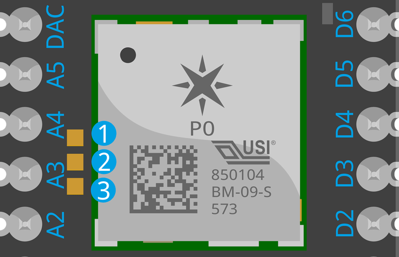
These pads would be used for the external coexistent interface to prevent simultaneous transmission on with an external radio, such as Bluetooth, while the Wi-Fi radio is transmitting. However the Wi-Fi radio software that runs on the P0, Broadcom/Cypress WICED, never supported this feature, so it cannot be enabled.
Memory map
STM32F205RGY6 Flash layout overview
- Bootloader (16 KB)
- DCT1 (16 KB), stores Wi-Fi credentials, keys, mfg info, system flags, etc..
- DCT2 (16 KB), swap area for DCT1
- EEPROM emulation bank 1 (16 KB)
- EEPROM emulation bank 2 (64 KB)
- Device OS (512 KB) [256 KB Wi-Fi/comms + 256 KB hal/platform/services]
- Factory backup, OTA backup and user application (384 KB) [3 x 128 KB]
DCT Layout
The DCT area of flash memory has been mapped to a separate DFU media device so that we can incrementally update the application data. This allows one item (say, server public key) to be updated without erasing the other items.
DCT layout in release/stable found here in firmware.
| Region | Offset | Size |
|---|---|---|
| system flags | 0 | 32 |
| version | 32 | 2 |
| device private key | 34 | 1216 |
| device public key | 1250 | 384 |
| ip config | 1634 | 120 |
| feature flags | 1754 | 4 |
| country code | 1758 | 4 |
| claim code | 1762 | 63 |
| claimed | 1825 | 1 |
| ssid prefix | 1826 | 26 |
| device code | 1852 | 6 |
| version string | 1858 | 32 |
| dns resolve | 1890 | 128 |
| reserved1 | 2018 | 64 |
| server public key | 2082 | 768 |
| padding | 2850 | 2 |
| flash modules | 2852 | 100 |
| product store | 2952 | 24 |
| antenna selection | 2976 | 1 |
| cloud transport | 2977 | 1 |
| alt device public key | 2978 | 128 |
| alt device private key | 3106 | 192 |
| alt server public key | 3298 | 192 |
| alt server address | 3490 | 128 |
| device id | 3618 | 12 |
| radio flags | 3630 | 1 |
| mode button mirror | 3631 | 32 |
| led mirror | 3663 | 96 |
| led theme | 3759 | 64 |
| reserved2 | 3823 | 435 |
Memory map (common)
| Region | Start Address | End Address | Size |
|---|---|---|---|
| Bootloader | 0x8000000 | 0x8004000 | 16 KB |
| DCT1 | 0x8004000 | 0x8008000 | 16 KB |
| DCT2 | 0x8008000 | 0x800C000 | 16 KB |
| EEPROM1 | 0x800C000 | 0x8010000 | 16 KB |
| EEPROM2 | 0x8010000 | 0x8020000 | 64 KB |
Memory map (modular firmware - default)
| Region | Start Address | End Address | Size |
|---|---|---|---|
| System Part 1 | 0x8020000 | 0x8060000 | 256 KB |
| System Part 2 | 0x8060000 | 0x80A0000 | 256 KB |
| User Part | 0x80A0000 | 0x80C0000 | 128 KB |
| OTA Backup | 0x80C0000 | 0x80E0000 | 128 KB |
| Factory Backup | 0x80E0000 | 0x8100000 | 128 KB |
Memory map (monolithic firmware - optional)
| Region | Start Address | End Address | Size |
|---|---|---|---|
| Firmware | 0x8020000 | 0x8080000 | 384 KB |
| Factory Reset | 0x8080000 | 0x80E0000 | 384 KB |
| Unused (factory reset modular) | 0x80E0000 | 0x8100000 | 128 KB |
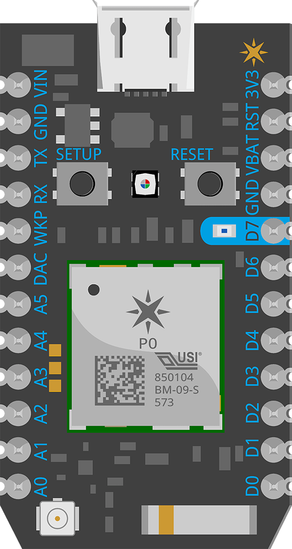
Pin and button definition
Pin markings
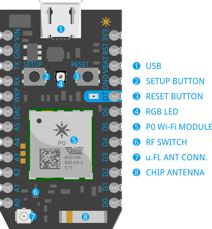
Pin description
| Pin | Description |
|---|---|
| VIN | This pin can be used as an input or output. As an input, supply 3.6 to 5.5VDC to power the Photon. When the Photon is powered via the USB port, this pin will output a voltage of approximately 4.8VDC due to a reverse polarity protection series Schottky diode between VUSB and VIN. When used as an output, the max load on VIN is 1A. |
| RST | Active-low reset input. On-board circuitry contains a 1k ohm pull-up resistor between RST and 3V3, and 0.1uF capacitor between RST and GND. |
| VBAT | Supply to the internal RTC, backup registers and SRAM when 3V3 is not present (1.65 to 3.6VDC). |
| 3V3 | This pin is the output of the on-board regulator and is internally connected to the VDD of the Wi-Fi module. When powering the Photon via VIN or the USB port, this pin will output a voltage of 3.3VDC. This pin can also be used to power the Photon directly (max input 3.3VDC). When used as an output, the max load on 3V3 is 100mA. NOTE: When powering the Photon via this pin, ensure power is disconnected from VIN and USB. |
| RX | Primarily used as UART RX, but can also be used as a digital GPIO or PWM[2]. |
| TX | Primarily used as UART TX, but can also be used as a digital GPIO or PWM[2]. |
| WKP | Active-high wakeup pin, wakes the module from sleep/standby modes. When not used as a WAKEUP, this pin can also be used as a digital GPIO, ADC input or PWM[2]. Can be referred to as A7 when used as an ADC. |
| DAC | 12-bit Digital-to-Analog (D/A) output (0-4095), referred to as DAC or DAC1 in software. Can also be used as a digital GPIO or ADC. Can be referred to as A6 when used as an ADC. A3 is a second DAC output used as DAC2 in software. |
| A0~A7 | 12-bit Analog-to-Digital (A/D) inputs (0-4095), and also digital GPIOs. A6 and A7 are code convenience mappings, which means pins are not actually labeled as such but you may use code like analogRead(A7). A6 maps to the DAC pin and A7 maps to the WKP pin. A4,A5,A7 may also be used as a PWM[2] output. |
| D0~D7 | Digital only GPIO pins. D0~D3 may also be used as a PWM[2] output. |
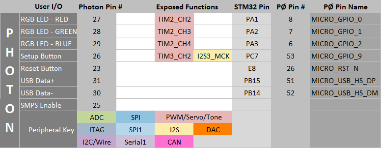
Notes: [1] In addition to the 24 pins around the outside of the Photon, there are 7 pads on the bottom the Photon PCB that can be used to connect to extra signals: RGB LED outputs, SETUP button, SMPS enable line and USB D+/D-. Photon Pins #25-31 are described in the Pin out diagrams. Also refer to the Recommended PCB land pattern photon without headers section for their location on the bottom of the Photon.
[2] PWM is available on D0, D1, D2, D3, A4, A5, WKP, RX, TX with a caveat: PWM timer peripheral is duplicated on two pins (A5/D2) and (A4/D3) for 7 total independent PWM outputs. For example: PWM may be used on A5 while D2 is used as a GPIO, or D2 as a PWM while A5 is used as an analog input. However A5 and D2 cannot be used as independently controlled PWM outputs at the same time.
Pinout diagrams

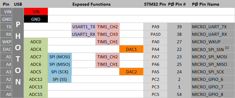
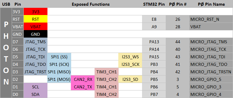
Notes:
[1] MICRO_SPI_SSN is only for reference as a PØ module pin name. It is technically speaking the STM32 pin PA4 which is the SS pin in an hardware SPI driven sense, however in the Particle API SPI SS is only user controlled as a GPIO. The hardware SS pin is not implemented. The default SS pin for the Particle SPI API is A2 (STM32 pin PC2), but any GPIO can be used for this function with SPI.begin(pin).
Technical specification
Absolute maximum ratings
| Parameter | Symbol | Min | Typ | Max | Unit |
|---|---|---|---|---|---|
| Supply Input Voltage | VVIN-MAX | +6.5 | V | ||
| Supply Output Current | IVIN-MAX-L | 1 | A | ||
| Supply Output Current | I3V3-MAX-L | 100 | mA | ||
| Storage Temperature | Tstg | -40 | +85 | °C | |
| Enable Voltage | VEN | VVIN+0.6 | V | ||
| ESD Susceptibility HBM (Human Body Mode) | VESD | 2 | kV |
Recommended operating conditions
| Parameter | Symbol | Min | Typ | Max | Unit |
|---|---|---|---|---|---|
| Supply Input Voltage | VVIN | +3.6 | +5.5 | V | |
| Supply Input Voltage | V3V3 | +3.0 | +3.3 | +3.6 | V |
| Supply Output Voltage | VVIN | +4.8 | V | ||
| Supply Output Voltage | V3V3 | +3.3 | V | ||
| Supply Input Voltage | VVBAT | +1.65 | +3.6 | V | |
| Supply Input Current (VBAT) | IVBAT | 19 | uA | ||
| Operating Current (Wi-Fi on) | IVIN avg | 80 | 100 | mA | |
| Operating Current (Wi-Fi on) | IVIN pk | 235[1] | 430[1] | mA | |
| Operating Current (Wi-Fi on, w/powersave) | IVIN avg | 18 | 100[2] | mA | |
| Operating Current (Wi-Fi off) | IVIN avg | 30 | 40 | mA | |
| Sleep Current (5V @ VIN) | IQs | 1 | 2 | mA | |
| Deep Sleep Current (5V @ VIN) | IQds | 80 | 100 | uA | |
| Operating Temperature | Top | -20 | +60 | °C | |
| Humidity Range Non condensing, relative humidity | 95 | % |
Notes:
[1] These numbers represent the extreme range of short peak current bursts when transmitting and receiving in 802.11b/g/n modes at different power levels. Average TX current consumption in will be 80-100mA.
[2] These are very short average current bursts when transmitting and receiving. On average if minimizing frequency of TX/RX events, current consumption in powersave mode will be 18mA
Power consumption
| Parameter | Symbol | Min | Typ | Peak | Unit |
|---|---|---|---|---|---|
| Operating Current (uC on, peripherals and radio disabled) | Iidle | 53.3 | 54.6 | 55.7 | mA |
| Operating Current (uC on, Wi-Fi on but not connected) | Iwifi_idle | 32.1 | 60.4 | 302 | mA |
| Operating Current (uC on, Wi-Fi connecting to ap) | Iwifi_conn_ap | 88.3 | 103 | 308 | mA |
| Operating Current (uC on, Wi-Fi connecting to cloud) | Iwifi_conn_cloud | 79.8 | 94.5 | 270 | mA |
| Operating Current (uC on, Wi-Fi connected but idle) | Iwifi_cloud_idle | 89.9 | 106 | 296 | mA |
| Operating Current (uC on, Wi-Fi connected and transmitting) | Iwifi_cloud_tx | 80.2 | 107 | 294 | mA |
| STOP mode sleep, GPIO wake-up | Istop_gpio | 2.15 | 2.75 | 3.26 | mA |
| STOP mode sleep, analog wake-up | Istop_analog | 6.66 | 7.56 | 8.45 | mA |
| STOP mode sleep, RTC wake-up | Istop_intrtc | 2.11 | 2.82 | 3.39 | mA |
| STOP mode sleep, serial wake-up | Istop_usart | 16.7 | 18.2 | 21.6 | mA |
| ULP mode sleep, GPIO wake-up | Iulp_gpio | 2.14 | 2.76 | 3.24 | mA |
| ULP mode sleep, RTC wake-up | Iulp_intrtc | 2.11 | 2.83 | 3.33 | mA |
| HIBERNATE mode sleep, GPIO wake-up | Ihib_gpio | 45.0 | 114 | 319 | uA |
| HIBERNATE mode sleep, RTC wake-up | Ihib_rtc | 44.7 | 114 | 319 | uA |
1The min, and particularly peak, values may consist of very short transients. The typical (typ) values are the best indicator of overall power consumption over time. The peak values indicate the absolute minimum capacity of the power supply necessary, not overall consumption.
Wi-Fi Specifications
| Feature | Description | |
|---|---|---|
| WLAN Standards | IEEE 802 11b/g/n | |
| Antenna Port | Single Antenna | |
| Frequency Band | 2.412GHz -- 2.462GHz (United States of America and Canada) | |
| 2.412GHz -- 2.472GHz (EU/Japan) | ||
| Sub Channels | 1 -- 11 (United States of America and Canada) | |
| 1 -- 13 (EU/Japan) | ||
| Modulation | DSSS, CCK, OFDM, BPSK, QPSK, 16QAM, 64QAM |
| PØ module Wi-Fi output power | Typ. | Tol. | Unit | |
|---|---|---|---|---|
| RF Average Output Power, 802.11b CCK Mode | 1M | Avail. upon request | +/- 1.5 | dBm |
| 11M | - | +/- 1.5 | dBm | |
| RF Average Output Power, 802.11g OFDM Mode | 6M | - | +/- 1.5 | dBm |
| 54M | - | +/- 1.5 | dBm | |
| RF Average Output Power, 802.11n OFDM Mode | MCS0 | - | +/- 1.5 | dBm |
| MCS7 | - | +/- 1.5 | dBm |
I/O characteristics
These specifications are based on the STM32F205RGY6 datasheet, with reference to Photon pin nomenclature.
| Parameter | Symbol | Conditions | Min | Typ | Max | Unit |
|---|---|---|---|---|---|---|
| Standard I/O input low level voltage | VIL | -0.3 | 0.28*(V3V3-2)+0.8 | V | ||
| I/O FT[1] input low level voltage | VIL | -0.3 | 0.32*(V3V3-2)+0.75 | V | ||
| Standard I/O input high level voltage | VIH | 0.41*(V3V3-2)+1.3 | V3V3+0.3 | V | ||
| I/O FT[1] input high level voltage | VIH | V3V3 > 2V | 0.42*(V3V3-2)+1 | 5.5 | V | |
| VIH | V3V3 ≤ 2V | 0.42*(V3V3-2)+1 | 5.2 | V | ||
| Standard I/O Schmitt trigger voltage hysteresis[2] | Vhys | 200 | mV | |||
| I/O FT Schmitt trigger voltage hysteresis[2] | Vhys | 5% V3V3[3] | mV | |||
| Input/Output current max | Iio | ±25 | mA | |||
| Input/Output current total | Iio total | ±120 | mA | |||
| Input leakage current[4] | Ilkg | GND ≤ Vio ≤ V3V3 GPIOs | ±1 | µA | ||
| Input leakage current[4] | Ilkg | RPU | Vio = 5V, I/O FT | 3 | µA | |
| Weak pull-up equivalent resistor[5] | RPU | Vio = GND | 30 | 40 | 50 | k Ω |
| Weak pull-down equivalent resistor[5] | RPD | Vio = V3V3 | 30 | 40 | 50 | k Ω |
| I/O pin capacitance | CIO | 5 | pF | |||
| DAC output voltage (buffers enabled by default) | VDAC | 0.2 | V3V3-0.2 | V | ||
| DAC output resistive load (buffers enabled by default) | RDAC | 5 | k Ω | |||
| DAC output capacitive load (buffers enabled by default) | CDAC | 50 | pF |
Notes:
[1] FT = Five-volt tolerant. In order to sustain a voltage higher than V3V3+0.3 the internal pull-up/pull-down resistors must be disabled.
[2] Hysteresis voltage between Schmitt trigger switching levels. Based on characterization, not tested in production.
[3] With a minimum of 100mV.
[4] Leakage could be higher than max. if negative current is injected on adjacent pins.
[5] Pull-up and pull-down resistors are designed with a true resistance in series with switchable PMOS/NMOS. This PMOS/NMOS contribution to the series resistance is minimum (~10% order).
Mechanical specifications
Dimensions and weight
| Headers | Dimensions in inches (mm) | Weight |
|---|---|---|
| With | 1.44 x 0.8 x 0.27 (36.58 x 20.32 x 6.86) | 5 grams |
| Without | 1.44 x 0.8 x 0.17 (36.58 x 20.32 x 4.32) | 3.7 grams |
Mating connectors
The Photon (with headers) can be mounted with (qty 2) 12-pin single row 0.1" female headers. Typically these are 0.335" (8.5mm) tall, but you may pick a taller one if desired. When you search for parts like these it can be difficult to navigate the thousands of parts available online so here are a few good choices for the Photon:
| Description | MFG | MFG Part Number | Distributor |
|---|---|---|---|
| 12-pin 0.1" Female Header (Tin) | Sullins Connector Solutions | PPTC121LFBN-RC | Digi-Key |
| 12-pin 0.1" Female Header (Gold) | Sullins Connector Solutions | PPPC121LFBN-RC | Digi-Key |
| 12-pin 0.1" Female Header (Tin) | Harwin | M20-7821246 | Mouser |
You may also use other types, such as reverse mounted (bottom side SMT) female headers, low profile types, etc..
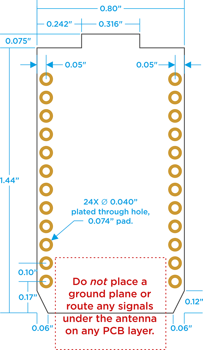
Recommended PCB land pattern (Photon with headers)
The Photon (with headers) can be mounted with 0.1" 12-pin female header receptacles using the following PCB land pattern:
A Photon with headers part for EAGLE can be found in the Particle EAGLE library
Recommended PCB land pattern (Photon without headers)
The Photon (without headers) can be surface mounted directly in an end application PCB using the following PCB land pattern:
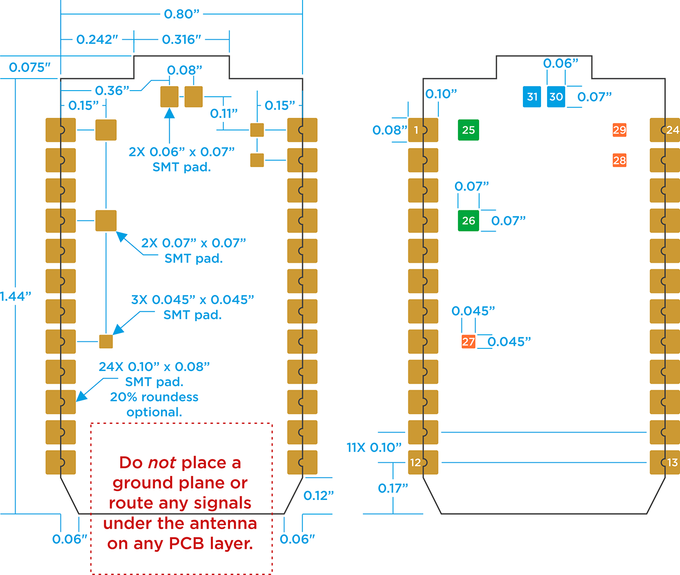
In addition to the 24 pins around the outside of the Photon, there are 7 pads on the bottom the Photon PCB that can be used to connect to extra signals: RGB LED outputs, SETUP button, SMPS enable line and USB D+/D-. Photon Pins #25-31 are described in the Pin out diagrams.
Solder mask around exposed copper pads should be 0.1mm (4 mils) larger in all directions. E.g., a 0.08" x 0.10" pad would have a 0.088" x 0.108" solder mask.
A Photon without headers part for EAGLE can be found in the Particle EAGLE library
Schematic
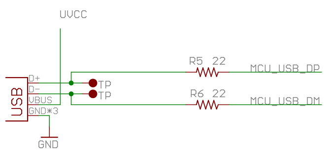
Schematic - USB
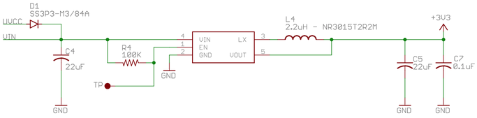
Schematic - Power
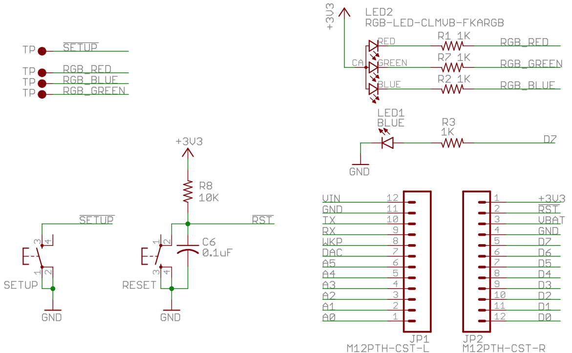
Schematic - User I/O
Schematic - RF
Schematic - PØ Wi-Fi module
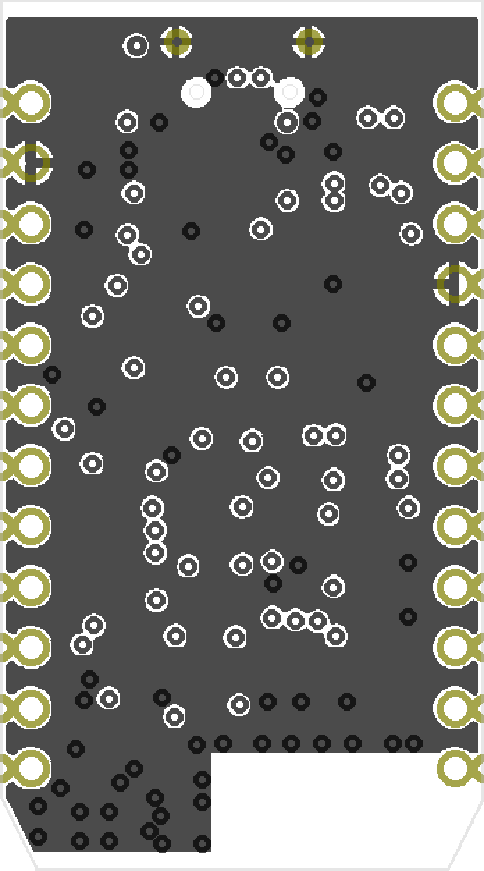
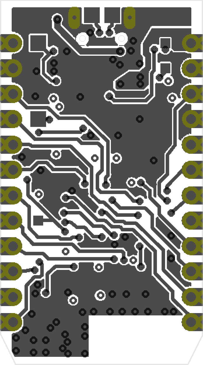
Layout
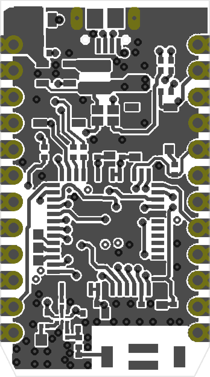
Photon v1.0.0 top layer (gtl)
Photon v1.0.0 GND layer (g2l)
Photon v1.0.0 3V3 layer (g15l)
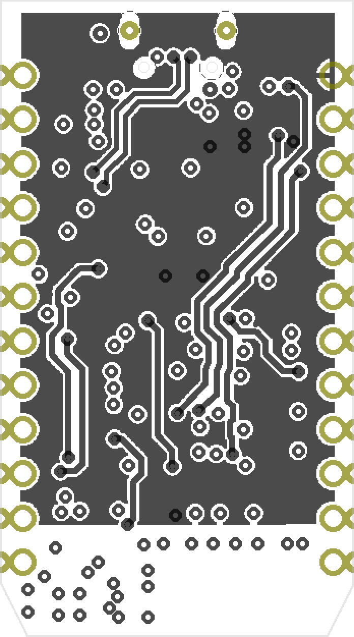
Photon v1.0.0 bottom layer (gbl)
Recommended solder reflow profile
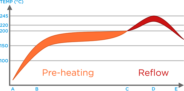
| Phase | Temperatures and Rates |
|---|---|
| A-B. | Ambient - 150°C, Heating rate: < 3°C/s |
| B-C. | 150 - 200°C, soak time: 60 - 120 s |
| C-D. | 200 - 245°C, Heating rate: < 3°C/s |
| D. | Peak temp.: 235 - 245°C, Time above 220°C: 40 - 90 s |
| D-E. | 245 - 220°C, Cooling rate: < 1°C/s |
Bill of materials
Build your own design based on the photon!
| Qty | Device | Minimum Specification | Package/Case | Part Designator | MFG. | MFG. PN |
|---|---|---|---|---|---|---|
| 1 | ANTENNA | 2.4GHz Ceramic | 5.0mm × 2.0mm x 2.6mm | ANT1 | Advanced Ceramic X | AT7020-E3R0HBA |
| 2 | CERAMIC CAPACITOR | 22uF Ceramic 6.3V 10% X5R | 0603 | C4,C5 | Samsung | CL10A226MQ8NRNC |
| 6 | CERAMIC CAPACITOR | 0.1uF Ceramic 6.3V 10% X5R | 0402 | C6,C7,C8,C11,C12,C16 | RongFu | 0402B104K01A |
| 2 | CERAMIC CAPACITOR | 100pF Ceramic 6.3V 10% X5R | 0402 | C2,C3 | Fenghua | 0402CG101J500NT |
| 4 | CERAMIC CAPACITOR | 10uF Ceramic 6.3V 10% X5R | 0603 | C9,C11,C13,C15 | Sumsung | CL10A106MQ8NNNC |
| 3 | CERAMIC CAPACITOR (RF) | 10pF Ceramic 6.3V 10% X5R | 0402 | C1,C14,C17 | Murata | GJM1555C1HR80BB01D |
| 1 | CONNECTOR | USB Micro-B w/tabs & slots | USB-MICROB | X1 | Kaweei | CMCUSB-5BFM2G-01-D |
| 1 | CONNECTOR | uFL Connector | SMD | X2 | Kaweei | P1163-0140R |
| 2 | HEADER | Single String 1.2" Mating Length | 0.1" 12-pin | JP1,JP2 | Kaweei | CP25411-12G-S116-A |
| 1 | DIODE | Diode Schottky 30V 3A | DO-220AA | D1 | Vishay | SS3P3-M3/84A |
| 1 | DIODE (LED) | Blue | SMD 0603 | LED1 | Everlight | 19-217/BHC-ZL1M2RY/3T |
| 1 | DIODE (LED) | LED RGB Common Anode Diffused SMD | 4-PLCC (2.0mm x 2.0mm) | LED2 | Cree | CLMVB-FKA-CFHEHLCBB7A363 |
| 1 | INDUCTOR | 2.2uH 1.5A | 3mm x 3mm | L4 | Taiyo Yuden | NR3015T2R2M |
| 1 | INDUCTOR (RF) | 3.9nH RF inductor | 0402 | L3 | Johanson | L-07C3N9SV6T |
| 1 | INDUCTOR (RF) | 4.7nH RF inductor | 0402 | L1 | Johanson | L-07C4N7SV6T |
| 1 | INDUCTOR (RF) | 6.8nH RF inductor | 0402 | L2 | Johanson | L-07C6N8JV6T |
| 1 | WI-FI + MCU | Broadcom Wi-FI + STM32F205RGY6 MCU | Custom USI SMD | U1 | USI | WM-N-BM-09-S |
| 1 | RF SWITCH | RF Switch SPDT | UQFN-6 (1x1mm) | U3 | Skyworks | SKY13350-385LF |
| 1 | POWER REGULATOR | 3.3V 1.5MHz 600mA High Efficiency PWM Step-Down DC/DC Converter | SOT23-5 | U2 | Richtek | RT8008-33GB |
| 1 | RESISTOR | 100k 5% | 0402 | R4 | Fenghua | RC-02W104FT |
| 2 | RESISTOR | 22R 5% | 0402 | R5,R6 | Fenghua | RC-02W220JT |
| 1 | RESISTOR | 10k 5% | 0402 | R8 | Fenghua | RC-02W103JT |
| 4 | RESISTOR | 1k 5% | 0402 | R1,R2,R3,R7 | Fenghua | RC-02W102JT |
| 2 | SWITCH | Button 160gf | 3.6mm x 3.1mm | SETUP,RESET | Haoyu | TS-1185A-C |
Ordering information
Photons are available from store.particle.io in single quantities with and without headers, and also included in different maker kits.
| SKU | Description | Region | Lifecycle | Replacement |
|---|---|---|---|---|
| PHNTRAYH | Photon with Headers, Tray [x50] | Global | Deprecated | |
| PHNTRAYNOH | Photon without Headers, Tray [x50] | Global | Deprecated | |
| PHOTONH | Photon with Headers, [x1] | Global | Deprecated | |
| PHOTONKIT | Photon with Headers Starter Kit, [x1] | Global | Deprecated | |
| PHOTONNOH | Photon without Headers, Dev board Kit [x1] | Global | Deprecated |
Qualification and approvals

Photon with Headers
- Model Number: PHOTONH
- RoHS
- CE
- FCC ID: 2AEMI-PHOTON
- ISED: 20127-PHOTON
Photon without Headers
- Model Number: PHOTONNOH
- RoHS
- CE
- FCC ID: 2AEMI-PHOTON
- ISED: 20127-PHOTON
Product handling
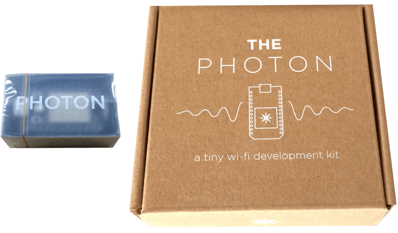
Packaging
The Photon comes in two primary styles of packaging: Matchbox and Kit Box. The matchbox packaging contains the bare essentials to get you started, while the Photon Kit contains a breadboard, Micro B USB cable, sticker, prototyping card and a couple sensors to build your first Internet connected project!
Photons without headers in matchbox packaging are also available in JEDEC style trays for automated pick and place machines. Request more details from us on this in the Contact section below.
Moisture sensitivity levels
The Moisture Sensitivity Level (MSL) relates to the packaging and handling precautions required. The PØ module on the Photons dominate the MSL requirements and are rated level 3. In general, this precaution applies for Photons without headers. If reflowing a Photon directly onto an application PCB, increased moisture levels prior to reflow can damage sensitive electronics on the Photon. A bake process to reduce moisture may be required.
For more information regarding moisture sensitivity levels, labeling, storage and drying see the MSL standard see IPC/JEDEC J-STD-020 (can be downloaded from www.jedec.org).
ESD precautions
The photon contains highly sensitive electronic circuitry and is an Electrostatic Sensitive Device (ESD). Handling a photon without proper ESD protection may destroy or damage it permanently. Proper ESD handling and packaging procedures must be applied throughout the processing, handling and operation of any application that incorporates photons. ESD precautions should be implemented on the application board where the photon is mounted. Failure to observe these precautions can result in severe damage to the photon!
Default settings
The Photon comes preprogrammed with a bootloader and a user application called Tinker. This application works with an iOS and Android app also named Tinker that allows you to very easily toggle digital pins, take analog and digital readings and drive variable PWM outputs.
The bootloader allows you to easily update the user application via several different methods, USB, OTA, Serial Y-Modem, and also internally via the Factory Reset procedure. All of these methods have multiple tools associated with them as well.
You may use the Particle Web IDE to code, compile and flash a user application OTA (Over The Air). Particle Workbench is a full-featured desktop IDE for Windows, Mac, and Linux based on VSCode and supports both cloud-based and local gcc-arm compiles. The Particle CLI provides a command-line interface for cloud-based compiles and flashing code over USB.
Glossary
FCC ISED CE warnings and end product labeling requirements
Federal Communication Commission Interference Statement This equipment has been tested and found to comply with the limits for a Class B digital device, pursuant to Part 15 of the FCC Rules. These limits are designed to provide reasonable protection against harmful interference in a residential installation. This equipment generates, uses and can radiate radio frequency energy and, if not installed and used in accordance with the instructions, may cause harmful interference to radio communications. However, there is no guarantee that interference will not occur in a particular installation. If this equipment does cause harmful interference to radio or television reception, which can be determined by turning the equipment off and on, the user is encouraged to try to correct the interference by one of the following measures:
- Reorient or relocate the receiving antenna.
- Increase the separation between the equipment and receiver.
- Connect the equipment into an outlet on a circuit different from that to which the receiver is connected.
- Consult the dealer or an experienced radio/TV technician for help.
FCC Caution: Any changes or modifications not expressly approved by the party responsible for compliance could void the user's authority to operate this equipment. This device complies with Part 15 of the FCC Rules. Operation is subject to the following two conditions:
- This device may not cause harmful interference, and
- This device must accept any interference received, including interference that may cause undesired operation.
FCC Radiation Exposure Statement: This equipment complies with FCC radiation exposure limits set forth for an uncontrolled environment. This transmitter module must not be co-located or operating in conjunction with any other antenna or transmitter. This End equipment should be installed and operated with a minimum distance of 20 centimeters between the radiator and your body.
IMPORTANT NOTE: In the event that these conditions can not be met (for example certain laptop configurations or co-location with another transmitter), then the FCC authorization is no longer considered valid and the FCC ID can not be used on the final product. In these circumstances, the OEM integrator will be responsible for re-evaluating the end product (including the transmitter) and obtaining a separate FCC authorization.
End Product Labeling The final end product must be labeled in a visible area with the following:
Contains FCC ID: 2AEMI-PHOTON
Manual Information to the End User The OEM integrator has to be aware not to provide information to the end user regarding how to install or remove this RF module in the user’s manual of the end product which integrates this module.
Canada Statement This device complies with Industry Canada’s licence-exempt RSSs. Operation is subject to the following two conditions:
- This device may not cause interference; and
- This device must accept any interference, including interference that may cause undesired operation of the device.
Le présent appareil est conforme aux CNR d’Industrie Canada applicables aux appareils radio exempts de licence.
L’exploitation est autorisée aux deux conditions suivantes:
- l’appareil ne doit pas produire de brouillage;
- l’utilisateur de l’appareil doit accepter tout brouillage radioélectrique subi, même si le brouillage est susceptible d’en compromettre le fonctionnement.
Caution Exposure: This device meets the exemption from the routine evaluation limits in section 2.5 of RSS102 and users can obtain Canadian information on RF exposure and compliance. Le dispositif répond à l'exemption des limites d'évaluation de routine dans la section 2.5 de RSS102 et les utilisateurs peuvent obtenir des renseignements canadiens sur l'exposition aux RF et le respect.
The final end product must be labelled in a visible area with the following: The Industry Canada certification label of a module shall be clearly visible at all times when installed in the host device, otherwise the host device must be labelled to display the Industry Canada certification number of the module, preceded by the words “Contains transmitter module”, or the word “Contains”, or similar wording expressing the same meaning, as follows:
Contains transmitter module ISED: 20127-PHOTON
This End equipment should be installed and operated with a minimum distance of 20 centimeters between the radiator and your body. Cet équipement devrait être installé et actionné avec une distance minimum de 20 centimètres entre le radiateur et votre corps.
The end user manual shall include all required regulatory information/warning as shown in this manual.
Revision history
| Revision | Date | Author | Comments |
|---|---|---|---|
| - | 30-March-2015 | BW | Initial release |
| v003 | 7-April-2015 | BW | Updated template |
| v004 | 8-April-2015 | BW | Updated Overview, Block diagram, Power, RF, and Pin markings sections |
| v005 | 9-April-2015 | BW | Updated BOM |
| v006 | 21-April-2015 | BW | Added JTAG, BT CO-EX, I/O Characteristics, Schematic, Layout, Reflow Profile, Glossary, Updated Operating Conditions |
| v007 | 28-April-2015 | BW | Added Layout, Updated analog pins, Land patterns, Packaging, Mating Connectors |
| v008 | 11-May-2015 | BW | Updated BT CO-EX, PWM info, Qualifications |
| v009 | 31-May-2015 | BW | Updated Pinouts, DAC info, Height dimensions, Solder mask info, Recommended operating conditions |
| v010 | 1-June-2015 | BW | Updated VBAT info |
| v011 | 24-July-2015 | BW | Added FCC ISED CE Warnings and End Product Labeling Requirements, Updated power output, added approved antennas, Corrected DAC2 as A3, Added pin numbers to PCB Land Pattern for Photon without headers. |
| v012 | 15-January-2016 | WH | Added TELEC Certification information and expanded explanation of Photons with and without headers. |
| v013 | 7-April-2016 | BW | Added: full STM32 part number, Memory map, DAC limits, SWD pin locations, max source/sink current, more descriptive info about bottom side pads, known errata URL. Updated: BT COEX info, pin diagram, block diagram, operating conditions, pin descriptions, land-pattern image signal keepout note. |
| v014 | 13-September-2016 | BW | Updated Mating connectors section. |
| v015 | 25-July-2017 | BW | Updated the Pin Description section and added high resolution pinout PDF, PWM notes and DCT layout, added warning to power section |
| v016 | 31-May-2018 | BW | Updated External Coexistence Interface section (unsupported) |
| v017 | 16-Sep-2020 | RK | Added power consumption information |
| v018 | 15-Mar-2021 | RK | Updated ordering information |
| v019 | 19-May-2021 | RK | Updated External Coexistence Interface section |
| v020 | 10-Sep-2021 | RK | Changed wording of peak vs. max current |
| v021 | 14-Mar-2023 | RK | Added deprecation notice |
| v022 | 31-Jan-2023 | RK | Added Device OS versions |
Known errata
We are tracking known errata with this datasheet here. These issues/errors in the datasheet will be resolved in subsequent revisions.
Contact
Web
https://www.particle.io
Community Forums
https://community.particle.io