
Photon 2 Datasheet
Functional description
Overview
The Photon 2 is a development module with a microcontroller and Wi-Fi networking. The form-factor is similar to the Argon (Adafruit Feather), but the Photon 2 supports 2.4 GHz and 5 GHz Wi-Fi, BLE, and has much larger RAM and flash that can support larger applications.
It is intended to replace both the Photon and Argon modules. It contains the same module as the P2, making it easier to migrate from a pin-based development module to a SMD mass-production module if desired.
Features
- 802.11a/b/g/n Wi-Fi, 2.4 GHz and 5 GHz
- Integrated PCB antenna
- Integrated U.FL connector for external antenna
- Integrated RF switch
- BLE 5 using same antenna as Wi-Fi
- Realtek RTL8721DM MCU
- ARM Cortex M33 CPU, 200 MHz
- 2048 KB (2 MB) user application maximum size
- 3072 KB (3 MB) of RAM available to user applications
- 2 MB flash file system
- FCC (United States), ISED (Canada), and CE (European Union) certified
Device OS Support
The Photon 2 and P2 require Device OS 5.0.0 or later. It is recommended that you use the latest version in the 5.x release line.
For information on upgrading Device OS, see Version information. For the latest version shipped from the factory, see Manufacturing firmware versions page. See also Long Term Support (LTS) releases.
Interfaces
Block diagram
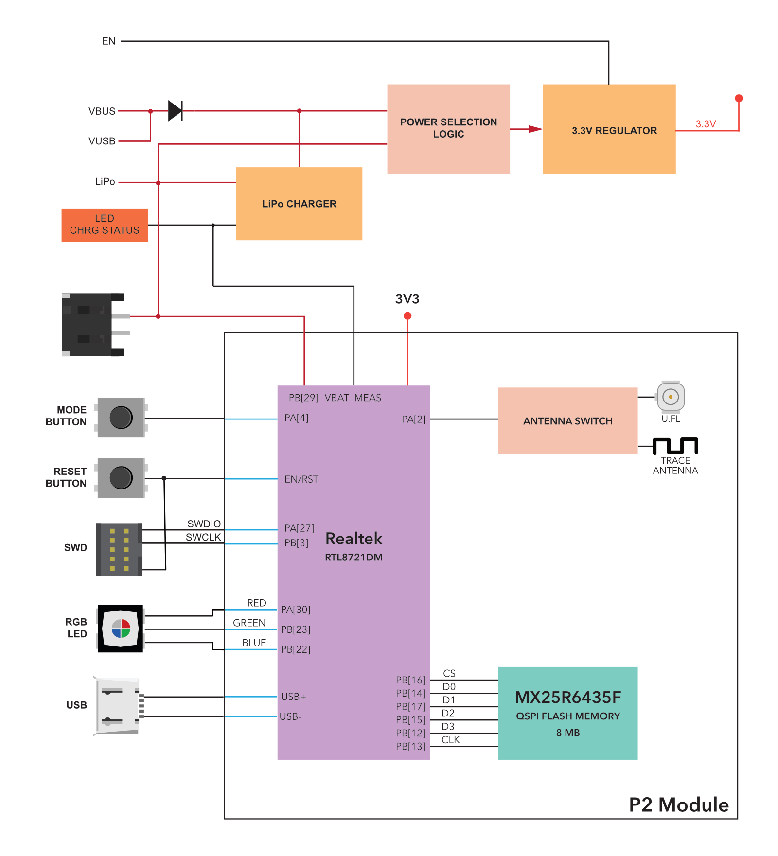
Power
USB
The USB port is the easiest way to power up the Photon 2. Please make sure that the USB port is able to provide at least 500mA. The Photon 2 has a micro B connector, same as the Photon.
VUSB Pin
The pin is internally connected to the VBUS of the USB port. The nominal output should be around 4.5 to 5 VDC when the device is plugged into the USB port and 0 when not connected to a USB source. You can use this pin to power peripherals that operate at such voltages. Do not exceed the current rating of the USB port, which is nominally rated to 500mA. This pin is also protected with an internal fuse rated at 1000mA.
It is also possible to use the VUSB to power the Photon 2 at 5V if not using the USB port. There is no blocking diode between the USB port and VUSB, so you should not use both at the same time.
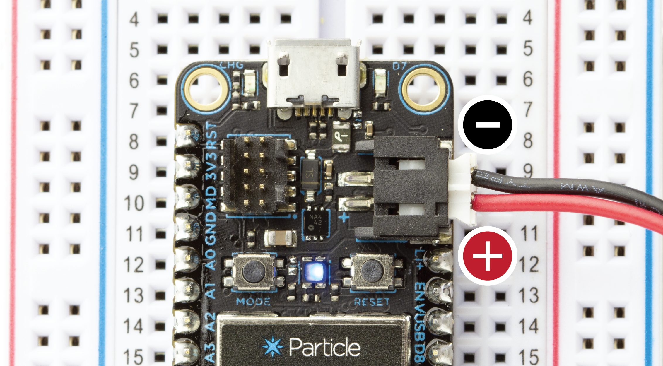
LiPo
If you want to make your projects truly wireless, you can power the device with a single cell LiPo (3.7V). The Photon 2 has an on board LiPo charger that will charge and power the device when USB source is plugged in or power the device from the LiPo alone in the absence of the USB.
NOTE: Please pay attention to the polarity of the JST-PH LiPo connector. Not all LiPo batteries follow the same polarity convention!
Li+ pin
This pin is internally connected to the positive terminal of the LiPo connector. You can connect a single cell LiPo/Lithium Ion or a DC supply source to this pin for powering the Photon 2. Remember that the input voltage range on this pin is 3.6 to 4.2 VDC.
3V3 PIN
This pin is the output of the on board 3.3V step-down switching regulator. The regulator is rated at 500mA max. When using this pin to power other devices or peripherals remember to budget in the current requirement of the Photon 2 first. Unlike the Photon, this pin CANNOT be used to power the Photon 2.
EN pin
The EN pin is not a power pin, per se, but it controls the 3V3 power. The EN pin is pulled high by a 100K resistor to the higher of VUSB, the micro USB connector, or Li+. Because the pull-up can result in voltages near 5V you should never directly connect EN to a 3.3V GPIO pin. Instead, you should only pull EN low, such as by using an N-channel MOSFET or other open-collector transistor.
The EN pin can force the device into a deep power-down state where it uses very little power. It also can used to assure that the device is completely reset, similar to unplugging it, with one caveat:
If using the EN pin to deeply reset the device, you must be careful not to allow leakage current back into the MCU by GPIO or by pull-ups to 3V3. If you only power external devices by 3V3 you won't run into this, as 3V3 is de-powered when EN is low.
However, if you have circuitry that is powered by a separate, external power supply, you must be careful. An externally powered circuit that drives a GPIO high when EN is low can provide enough current to keep the MCU from powering down and resetting. Likewise, a pull-up to an external power supply can do the same thing. Be sure that in no circumstances can power by supplied to the MCU when 3V3 is de-powered.
Antenna
- The Photon 2 includes an on-module PCB trace antenna and a U.FL connector that allows the user to connect an external antenna.
- The antenna is selected in software. The default is the PCB trace antenna.
- A single antenna is used for both Wi-Fi and BLE.
Approved antennas
In addition to the built-in trace antenna, the following optional external antenna is certified for use with the Photon 2:
| Antenna | SKU |
|---|---|
| Particle P2/Photon2 Wi-Fi Antenna 2.4/5GHz, [x1] | PARANTWM1EA |
| Particle P2/Photon2 Wi-Fi Antenna 2.4/5GHz, [x50] | PARANTWM1TY |
This antenna is used for both Wi-Fi and BLE. In order to use an external antenna, it must be selected in software.
A different dual-band antenna can be used but this will likely require both intentional and unintentional radiator certification.
Do not use the Argon Wi-Fi/BLE antenna (ANT-FLXV2) on the P2, Photon 2, or M-SoM. The Argon antenna does not work with 5 GHz and this will result in poor Wi-Fi performance on the P2, Photon 2, and M-SoM.
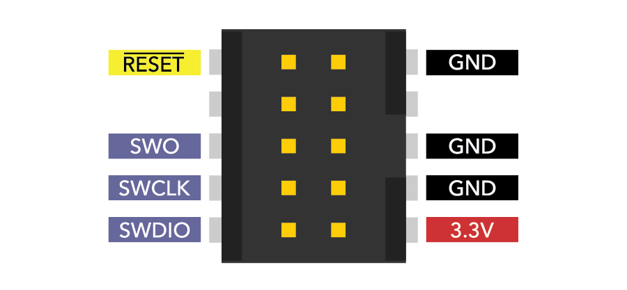
SWD/JTAG
The Photon 2 module supports programming and debugging use SWD (Serial Wire Debug) using the 10-pin micro JTAG connector on the top of the module.
When the bootloader starts, for a brief period of time a weak pull-up is applied to pin D8 and pull-down to pin D6 to detect whether a SWD debugger is attached. After boot, you can use these pins for regular GPIO, but beware of a possible GPIO state change caused by the pull-up or pull-down when using these pins as output.
| Pin | JTAG | MCU Pin | Pull at boot |
|---|---|---|---|
| D7 | SWDIO | PA[27] | Pull-up |
| D6 | SWCLK | PB[3] | Pull-down |
| 3V3 | Power | ||
| GND | Ground | ||
| RST | Reset |
LED status
System RGB LED
For a detailed explanation of different color codes of the RGB system LED, please take a look here.
Charge status LED
| State | Description |
|---|---|
| ON | Charging in progress |
| OFF | Charging complete |
Memory map
Flash layout overview
| Address | File | Purpose |
|---|---|---|
| 0x00000000 | p2-prebootloader-mbr | This file is factory configured and must never be overwritten |
| 0x00004000 | p2-bootloader | Device OS bootloader |
| 0x00014000 | p2-prebootloader-part1 | Bootloader for KM0 processor, infrequently modified |
| 0x00060000 | p2-system-part1 | Device OS system part |
The location of the user binary is dependent on the size of the user binary and is not flashed to a fixed location.
Do not chip erase the RTL872x under any circumstances! Also do not flash anything to address 0 (prebootloader-mbr). The prebootloader-mbr is factory configured for your specific device with the private keys necessary for secure boot. If you erase or overwrite this portion of the flash you will not be able to program or use the device again.
DCT Layout
The DCT area of flash memory has been mapped to a separate DFU media device so that we can incrementally update the application data. This allows one item (say, server public key) to be updated without erasing the other items.
| Region | Offset | Size |
|---|---|---|
| system flags | 0 | 32 |
| version | 32 | 2 |
| device private key | 34 | 1216 |
| device public key | 1250 | 384 |
| ip config | 1634 | 120 |
| feature flags | 1754 | 4 |
| country code | 1758 | 4 |
| claim code | 1762 | 63 |
| claimed | 1825 | 1 |
| ssid prefix | 1826 | 26 |
| device code | 1852 | 6 |
| version string | 1858 | 32 |
| dns resolve | 1890 | 128 |
| reserved1 | 2018 | 64 |
| server public key | 2082 | 768 |
| padding | 2850 | 2 |
| flash modules | 2852 | 100 |
| product store | 2952 | 24 |
| antenna selection | 2976 | 1 |
| cloud transport | 2977 | 1 |
| alt device public key | 2978 | 128 |
| alt device private key | 3106 | 192 |
| alt server public key | 3298 | 192 |
| alt server address | 3490 | 128 |
| device id | 3618 | 12 |
| radio flags | 3630 | 1 |
| mode button mirror | 3631 | 32 |
| led mirror | 3663 | 96 |
| led theme | 3759 | 64 |
| reserved2 | 3823 | 435 |
Pin and button definition
| Peripheral Type | Qty | Input(I) / Output(O) |
|---|---|---|
| Digital | 20 | I/O |
| Analog (ADC) | 6 | I |
| SPI | 2 | I/O |
| I2C | 1 | I/O |
| UART | 3 | I/O |
| USB | 1 | I/O |
| PWM | 5 | O |
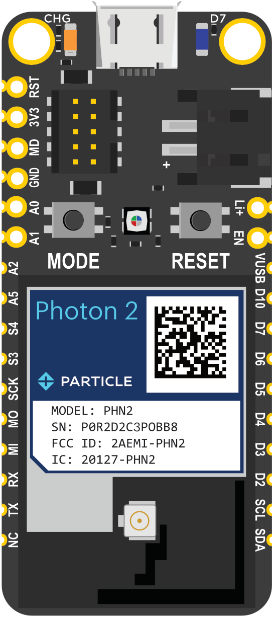
Pin markings

GPIO and port listing
| Pin Name | PWM | MCU | ||||
|---|---|---|---|---|---|---|
| A0 / D11 | ADC_4 | PB[1] | ||||
| A1 / D12 | ADC_5 | PB[2] | ||||
| A2 / D13 | ADC_3 | ✓ | PB[7] | |||
| A5 / D14 | ADC_0 | ✓ | PB[4] | |||
| D0 / A3 | ADC_2 | Wire (SDA) | PB[6] | |||
| D1 / A4 | ADC_1 | Wire (SCL) | ✓ | PB[5] | ||
| D2 | SPI1 (MOSI) | Serial2 (RTS) | PA[16] | |||
| D3 | SPI1 (MISO) | Serial2 (CTS) | PA[17] | |||
| D4 | SPI1 (SCK) | Serial2 (TX) | PA[18] | |||
| D5 | SPI1 (SS) | Serial2 (RX) | PA[19] | |||
| D6 | SWCLK | PB[3] | ||||
| D7 | SWDIO | PA[27] | ||||
| D10 / WKP | Serial3 (CTS) | PA[15] | ||||
| MISO / D16 | SPI (MISO) | Serial3 (RX) | ✓ | PA[13] | ||
| MOSI / D15 | SPI (MOSI) | Serial3 (TX) | ✓ | PA[12] | ||
| RX / D9 | Serial1 (RX) | PA[8] | ||||
| S3 / D18 | SPI (SS) | PB[26] | ||||
| S4 / D19 | PA[0] | |||||
| SCK / D17 | SPI (SCK) | Serial3 (RTS) | PA[14] | |||
| TX / D8 | Serial1 (TX) | PA[7] |
- The drive strength is 4 mA per pin in normal drive and 12 mA per pin in high drive mode on the Photon 2.
- Drive strength selection using pinSetDriveStrength is only available in Device OS 5.5.0 and later on the Photon 2.
- Pins TX, D6, and D7 have additional limitations, see boot mode pins, below.
ADC (analog to digital converter)
The Photon 2 supports six ADC inputs.
| Pin Name | Description | Interface | MCU |
|---|---|---|---|
| A0 / D11 | A0 Analog in, PDM CLK, GPIO | ADC_4 | PB[1] |
| A1 / D12 | A1 Analog in, PDM DAT, GPIO | ADC_5 | PB[2] |
| A2 / D13 | A2 Analog in, GPIO, PWM. | ADC_3 | PB[7] |
| A5 / D14 | A5 Analog in, GPIO, PWM, Was A3 on Gen 3. | ADC_0 | PB[4] |
| D0 / A3 | D0 GPIO, I2C SDA, A3 Analog In | ADC_2 | PB[6] |
| D1 / A4 | D1 GPIO, PWM, I2C SCL, A4 Analog In | ADC_1 | PB[5] |
- ADC inputs are single-ended and limited to 0 to 3.3V
- Resolution is 12 bits
The VBAT_MEAS pin is connected to Li+ on the Photon 2 and is used to measure the battery voltage by using analogRead(A6). The value returned is 0 - 4095 (inclusive, 12-bit) but represents voltage from 0 - 5 VDC, not 3.3V as is the case with the other ADC inputs.
UART serial
The Photon 2 supports three UART serial interfaces.
| Pin Name | Description | Interface | MCU |
|---|---|---|---|
| D2 | D2 GPIO, Serial2 RTS, SPI1 MOSI | Serial2 (RTS) | PA[16] |
| D3 | D3 GPIO, Serial2 CTS, SPI1 MISO | Serial2 (CTS) | PA[17] |
| D4 | D4 GPIO, Serial2 TX, SPI1 SCK | Serial2 (TX) | PA[18] |
| D5 | D5 GPIO, Serial2 RX, SPI1 SS | Serial2 (RX) | PA[19] |
| D10 / WKP | D10 GPIO. Serial3 CTS, WKP. Was D8/WKP on Gen 3. | Serial3 (CTS) | PA[15] |
| MISO / D16 | D16 GPIO, S1 GPIO, PWM, SPI MISO, Serial3 RX. | Serial3 (RX) | PA[13] |
| MOSI / D15 | D15 GPIO, S0 GPIO, PWM, SPI MOSI, Serial3 TX | Serial3 (TX) | PA[12] |
| RX / D9 | Serial1 RX (received data), GPIO | Serial1 (RX) | PA[8] |
| SCK / D17 | SPI SCK, D13 GPIO, S3 GPIO, Serial3 RTS | Serial3 (RTS) | PA[14] |
| TX / D8 | Serial1 TX (transmitted data), GPIO | Serial1 (TX) | PA[7] |
- The UART pins are 3.3V and must not be connected directly to a RS-232C port or to a 5V TTL serial port
- Hardware flow control is optional; if not used then the RTS and CTS pins can be used as regular GPIO
- Serial1 uses the RTL872x UART_LOG peripheral
- Serial2 uses the RTL872x HS_UART0 peripheral
- Serial3 uses the RTL872x LP_UART peripheral
- Supported baud rates: 110, 300, 600, 1200, 2400, 4800, 9600, 14400, 19200, 28800, 38400, 57600, 76800, 115200, 128000, 153600, 230400, 380400, 460800, 500000, 921600, 1000000, 1382400, 1444400, 1500000, 1843200, 2000000, 2100000, 2764800, 3000000, 3250000, 3692300, 3750000, 4000000, 6000000
SPI
The Photon 2 supports two SPI (serial peripheral interconnect) ports.
| Pin Name | Description | Interface | MCU |
|---|---|---|---|
| D2 | D2 GPIO, Serial2 RTS, SPI1 MOSI | SPI1 (MOSI) | PA[16] |
| D3 | D3 GPIO, Serial2 CTS, SPI1 MISO | SPI1 (MISO) | PA[17] |
| D4 | D4 GPIO, Serial2 TX, SPI1 SCK | SPI1 (SCK) | PA[18] |
| D5 | D5 GPIO, Serial2 RX, SPI1 SS | SPI1 (SS) | PA[19] |
| MISO / D16 | D16 GPIO, S1 GPIO, PWM, SPI MISO, Serial3 RX. | SPI (MISO) | PA[13] |
| MOSI / D15 | D15 GPIO, S0 GPIO, PWM, SPI MOSI, Serial3 TX | SPI (MOSI) | PA[12] |
| S3 / D18 | S3 GPIO, SPI SS, Was A5 on Gen 3. | SPI (SS) | PB[26] |
| SCK / D17 | SPI SCK, D13 GPIO, S3 GPIO, Serial3 RTS | SPI (SCK) | PA[14] |
- The SPI port is 3.3V and must not be connected directly to devices that drive MISO at 5V
- If not using a SPI port, its pins can be used as GPIO
- Any pins can be used as the SPI chip select
- Multiple devices can generally share a single SPI port
- SPI uses the RTL872x SPI1 peripheral (25 MHz maximum speed)
- SPI1 uses the RTL872x SPI0 peripheral (50 MHz maximum speed)
If you are using SPI, Device OS 5.3.1 or later is recommended. Prior to that version, SPI ran at half of the set speed, and SPI1 ran at double the set speed. Timing has also been improved for large DMA transfers; prior to 5.3.1, there could be 1 µs gaps for every 16 bytes of data transferred.
I2C
The Photon 2 supports one I2C (two-wire serial interface) port.
| Pin Name | Description | Interface | MCU |
|---|---|---|---|
| D0 / A3 | D0 GPIO, I2C SDA, A3 Analog In | Wire (SDA) | PB[6] |
| D1 / A4 | D1 GPIO, PWM, I2C SCL, A4 Analog In | Wire (SCL) | PB[5] |
- The I2C port is 3.3V and must not be connected directly a 5V I2C bus
- Maximum bus speed is 400 kHz
- External pull-up resistors are required for I2C
- If not using I2C, pins D0 and D1 can be used as GPIO
PDM
Pulse density modulation digital microphones can be used with the Microphone_PDM library and the Photon 2, but only on specific pins:
| Pin Name | Description | Interface | MCU |
|---|---|---|---|
| A0 / D11 | A0 Analog in, PDM CLK, GPIO | CLK | PB[1] |
| A1 / D12 | A1 Analog in, PDM DAT, GPIO | DAT | PB[2] |
Boot mode pins
These pins have a special function at boot. Beware when using these pins as input as they can trigger special modes in the MCU.
| Pin | Pin Name | Description | MCU |
|---|---|---|---|
| 15 | TX / D8 | Low at boot triggers ISP flash download | PA[7] |
| 22 | D6 | SWCLK. 40K pull-down at boot. | PB[3] |
| 23 | D7 | SWDIO. 40K pull-up at boot. Low at boot triggers MCU test mode. | PA[27] |
Battery and charge pins
The Photon 2 does not have a fuel gauge chip, however you can determine the voltage of the LiPo battery, if present.
float voltage = analogRead(A6) / 819.2;
The constant is from the ADC range (0 - 4095) mapped to the voltage from 0 - 5 VDC (the maximum supported on VBAT_MEAS).
The current Photon 2 hardware is unable to reliably read the CHG pin. In particular, if you have a Photon 2 powered by both
USB and battery and is charging, then unplug the USB power, the charge LED will turn off, but the CHG pin will not change
state.
5V tolerance
GPIO and all ports such as I2C, SPI, UART serial, etc. are not 5V tolerant.
BLE (Bluetooth LE)
BLE Central Mode on the P2 and Photon 2 is only supported in Device OS 5.1.0 and later. Earlier versions only supported BLE Peripheral Mode.
Sleep
The Photon 2 can wake from STOP or ULTRA_LOW_POWER sleep mode on any GPIO, RISING, FALLING, or CHANGE.
The Photon 2 can only wake from HIBERNATE sleep mode on certain pins, RISING, FALLING, or CHANGE.
Pin D10 WKP is the same module pin location as the Argon pin D8, which is also the WKP pin.
| Pin Name | Description | Interface | MCU |
|---|---|---|---|
| D2 | D2 GPIO, Serial2 RTS, SPI1 MOSI | Pin can wake from HIBERNATE sleep | PA[16] |
| D3 | D3 GPIO, Serial2 CTS, SPI1 MISO | Pin can wake from HIBERNATE sleep | PA[17] |
| D4 | D4 GPIO, Serial2 TX, SPI1 SCK | Pin can wake from HIBERNATE sleep | PA[18] |
| D5 | D5 GPIO, Serial2 RX, SPI1 SS | Pin can wake from HIBERNATE sleep | PA[19] |
| D10 / WKP | D10 GPIO. Serial3 CTS, WKP. Was D8/WKP on Gen 3. | Pin can wake from HIBERNATE sleep | PA[15] |
| MISO / D16 | D16 GPIO, S1 GPIO, PWM, SPI MISO, Serial3 RX. | Pin can wake from HIBERNATE sleep | PA[13] |
| MOSI / D15 | D15 GPIO, S0 GPIO, PWM, SPI MOSI, Serial3 TX | Pin can wake from HIBERNATE sleep | PA[12] |
| SCK / D17 | SPI SCK, D13 GPIO, S3 GPIO, Serial3 RTS | Pin can wake from HIBERNATE sleep | PA[14] |
The Photon 2 preserves the state of outputs during STOP or ULTRA_LOW_POWER sleep mode. In HIBERNATE, outputs are high-impedance.
Most pins can use INPUT_PULLUP or INPUT_PULLDOWN in sleep modes. The exception is HIBERNATE sleep mode where pin S4 can only use an external hardware pull-up or pull down.
| Pin Name | Description | Interface | MCU |
|---|---|---|---|
| S4 / D19 | S4 GPIO, Was A4 on Gen 3. | No internal pull up or pull down in HIBERNATE sleep mode. | PA[0] |
RAM
The P2 has 512 KB of static RAM (SRAM) and 4 MB of pseudo-static RAM (PSRAM).
Around 3072 KB (3 MB) of RAM is available for user applications. Heap allocations are made first from SRAM, then from PSRAM, as necessary.
Retained memory
The P2 and Photon 2 have limited support for retained memory in Device OS 5.3.1 and later:
Retained memory is preserved on RTL872x devices in the following cases:
| Case | Saved |
|---|---|
| When entering sleep modes | 5.3.1 and later |
| OTA firmware updates | 5.3.1 and later |
System.backupRamSync() |
5.3.1 and later |
System.reset() |
Not saved |
| Reset button or reset pin | Not saved |
| Every 10 seconds | 5.3.1 to 5.8.0 only |
Calling System.backupRamSync() will manually save the contents of retained memory to a dedicated flash page on the RTL872x processor and will be restored after the device is reset. You should avoid saving the data extremely frequently as it is slower than RAM and will cause flash wear and is relatively slow to execute.
Prior to Device OS 5.3.1, retained memory is not supported on RTL872x devices. The flash file system can be used, or you can use an external chip such as an I2C or SPI FRAM.
Retained memory is 3068 bytes.
Pins Photon 2 vs. P2
The pins on the Photon 2 map directly the pins with the same name on the P2.
| Photon 2 Pin Name | Photon 2 Description | P2 Pin Name | P2 Description | P2 Pin Number | MCU |
|---|---|---|---|---|---|
| A0 / D11 | A0 Analog in, PDM CLK, GPIO | A0 / D11 | A0 Analog in, PDM CLK, GPIO | 50 | PB[1] |
| A1 / D12 | A1 Analog in, PDM DAT, GPIO | A1 / D12 | A1 Analog in, PDM DAT, GPIO | 43 | PB[2] |
| A2 / D13 | A2 Analog in, GPIO, PWM. | A2 / D13 | A2 Analog in, PWM, GPIO | 49 | PB[7] |
| A5 / D14 | A5 Analog in, GPIO, PWM, Was A3 on Gen 3. | A5 / D14 | A5 Analog in, GPIO, PWM. | 23 | PB[4] |
| D0 / A3 | D0 GPIO, I2C SDA, A3 Analog In | D0 / A3 | D0 GPIO, I2C SDA, A3 Analog In | 36 | PB[6] |
| D1 / A4 | D1 GPIO, PWM, I2C SCL, A4 Analog In | D1 / A4 | D1 GPIO, PWM, I2C SCL, A4 Analog In | 35 | PB[5] |
| D10 / WKP | D10 GPIO. Serial3 CTS, WKP. Was D8/WKP on Gen 3. | D10 / WKP | D10 GPIO, Serial 3 CTS, WKP. (Was WKP/A7 on P1.) | 30 | PA[15] |
| D2 | D2 GPIO, Serial2 RTS, SPI1 MOSI | D2 | D2 GPIO, Serial2 RTS, SPI1 MOSI | 45 | PA[16] |
| D3 | D3 GPIO, Serial2 CTS, SPI1 MISO | D3 | D3 GPIO, Serial2 CTS, SPI1 MISO | 51 | PA[17] |
| D4 | D4 GPIO, Serial2 TX, SPI1 SCK | D4 | D4 GPIO, Serial2 TX, SPI1 SCK | 52 | PA[18] |
| D5 | D5 GPIO, Serial2 RX, SPI1 SS | D5 | D5 GPIO, Serial2 RX, SPI1 SS | 53 | PA[19] |
| D6 | D6 GPIO, SWCLK. | D6 | D6 GPIO, SWCLK | 55 | PB[3] |
| D7 | D7 GPIO, Blue LED, SWDIO | D7 | D7 GPIO, SWDIO | 54 | PA[27] |
| MISO / D16 | D16 GPIO, S1 GPIO, PWM, SPI MISO, Serial3 RX. | S1 / D16 | S1 GPIO, PWM, SPI MISO, Serial3 RX. (Was P1S1 on P1.) | 41 | PA[13] |
| MODE | MODE button, has internal pull-up | MODE | MODE button. Pin number constant is BTN. External pull-up required! | 46 | PA[4] |
| MOSI / D15 | D15 GPIO, S0 GPIO, PWM, SPI MOSI, Serial3 TX | S0 / D15 | S0 GPIO, PWM, SPI MOSI, Serial3 TX, I2S MCLK. (Was P1S0 on P1.) | 40 | PA[12] |
| RST | Hardware reset. Pull low to reset; can leave unconnected in normal operation. | RST | Hardware reset. Pull low to reset; can leave unconnected in normal operation. | 34 | CHIP_EN |
| RX / D9 | Serial1 RX (received data), GPIO | RX / D9 | Serial1 RX (received data), GPIO | 63 | PA[8] |
| S3 / D18 | S3 GPIO, SPI SS, Was A5 on Gen 3. | S3 / D18 | S3 GPIO, I2S TX. (Was P1S3 on P1.), SPI SS | 44 | PB[26] |
| S4 / D19 | S4 GPIO, Was A4 on Gen 3. | S4 / D19 | S4 GPIO, I2S RX. (Was P1S4 on P1.) | 47 | PA[0] |
| SCK / D17 | SPI SCK, D13 GPIO, S3 GPIO, Serial3 RTS | S2 / D17 | S2 GPIO, SPI SCK, Serial3 RTS. (Was P1S2 on P1.) | 42 | PA[14] |
| TX / D8 | Serial1 TX (transmitted data), GPIO | TX / D8 | Serial1 TX (transmitted data), GPIO | 64 | PA[7] |
Complete pin listing
| Pin Name | Description | MCU |
|---|---|---|
| RST | Hardware reset. Pull low to reset; can leave unconnected in normal operation. | CHIP_EN |
| 3V3 | Regulated 3.3V DC output, maximum load 500 mA | |
| MODE | MODE button, has internal pull-up | PA[4] |
| GND | Ground. | |
| A0 / D11 | A0 Analog in, PDM CLK, GPIO | PB[1] |
| A1 / D12 | A1 Analog in, PDM DAT, GPIO | PB[2] |
| A2 / D13 | A2 Analog in, GPIO, PWM. | PB[7] |
| A5 / D14 | A5 Analog in, GPIO, PWM, Was A3 on Gen 3. | PB[4] |
| S4 / D19 | S4 GPIO, Was A4 on Gen 3. | PA[0] |
| S3 / D18 | S3 GPIO, SPI SS, Was A5 on Gen 3. | PB[26] |
| SCK / D17 | SPI SCK, D13 GPIO, S3 GPIO, Serial3 RTS | PA[14] |
| MOSI / D15 | D15 GPIO, S0 GPIO, PWM, SPI MOSI, Serial3 TX | PA[12] |
| MISO / D16 | D16 GPIO, S1 GPIO, PWM, SPI MISO, Serial3 RX. | PA[13] |
| RX / D9 | Serial1 RX (received data), GPIO | PA[8] |
| TX / D8 | Serial1 TX (transmitted data), GPIO | PA[7] |
| D0 / A3 | D0 GPIO, I2C SDA, A3 Analog In | PB[6] |
| D1 / A4 | D1 GPIO, PWM, I2C SCL, A4 Analog In | PB[5] |
| D2 | D2 GPIO, Serial2 RTS, SPI1 MOSI | PA[16] |
| D3 | D3 GPIO, Serial2 CTS, SPI1 MISO | PA[17] |
| D4 | D4 GPIO, Serial2 TX, SPI1 SCK | PA[18] |
| D5 | D5 GPIO, Serial2 RX, SPI1 SS | PA[19] |
| D6 | D6 GPIO, SWCLK. | PB[3] |
| D7 | D7 GPIO, Blue LED, SWDIO | PA[27] |
| D10 / WKP | D10 GPIO. Serial3 CTS, WKP. Was D8/WKP on Gen 3. | PA[15] |
| VUSB | Power out (when powered by USB) 5 VDC at 1A maximum. Power in with limitations. | |
| EN | Power supply enable. Connect to GND to power down. Has internal weak (100K) pull-up. | |
| LI+ | Connected to JST PH LiPo battery connector. 3.7V in or out. |
Complete module pin details


Technical specification
Recommended operating conditions
| Parameter | Symbol | Min | Typ | Max | Unit |
|---|---|---|---|---|---|
| Operating Temperature | Top | -20 | +70 | °C | |
| Humidity Range Non condensing, relative humidity | 95 | % |
I/O Characteristics
| Parameter | Symbol | Min | Typ | Peak | Unit |
|---|---|---|---|---|---|
| Input-High Voltage | VIH | 2.0 | V | ||
| Input-Low Voltage | VIL | 0.8 | V | ||
| Output drive strength (normal drive) | 4 | mA | |||
| Output drive strength (high drive) | 12 | mA | |||
| Total output drive (all pins) | 200 | mA |
Power consumption
| Parameter | Symbol | Min | Typ | Peak | Unit |
|---|---|---|---|---|---|
| Operating Current (uC on, peripherals and radio disabled) | Iidle | 21.4 | 23.2 | 23.8 | mA |
| Operating Current (uC on, BLE advertising) | Ible_adv | 54.7 | 58.7 | 70.7 | mA |
| Operating Current (uC on, radio connected to access point) | Iwifi_conn_ap | 54.6 | 60.5 | 265 | mA |
| STOP mode sleep, GPIO wake-up | Istop_gpio | 492 | 549 | 608 | uA |
| STOP mode sleep, time wake-up | Istop_intrtc | 500 | 552 | 598 | uA |
| ULP mode sleep, GPIO wake-up | Iulp_gpio | 492 | 549 | 608 | uA |
| ULP mode sleep, time wake-up | Iulp_intrtc | 500 | 552 | 598 | uA |
| HIBERNATE mode sleep, GPIO wake-up | Ihib_gpio | 114 | 249 | uA | |
| HIBERNATE mode sleep, time wake-up | Ihib_intrtc | 114 | 253 | uA |
1The min, and particularly peak, values may consist of very short transients. The typical (typ) values are the best indicator of overall power consumption over time. The peak values indicate the absolute minimum capacity of the power supply necessary, not overall consumption.
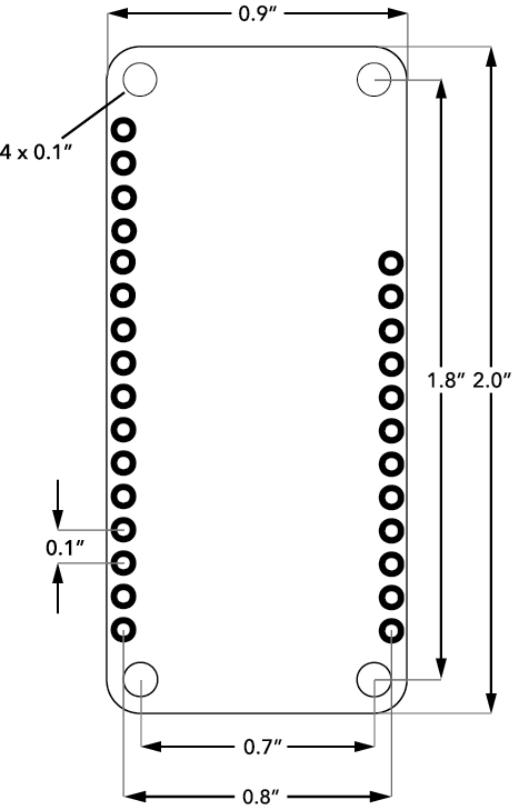
Mechanical specifications
Mating connectors
The Photon 2 uses two single row 0.1" pitch male header pins. One of them is 16 pin while the other is 12 pin. It can be mounted with matching 0.1" pitch female headers with a typical height of 0.335" (8.5mm). When you search for parts like these it can be difficult to navigate the thousands of parts available online so here are a few good choices for the Photon 2 and Argon:
| Description | MFG | MFG Part Number |
|---|---|---|
| 16-pin 0.1" (2.54mm) Female Header | Sullins | PPTC161LFBN-RC |
| 16-pin 0.1" (2.54mm) Female Header | TE | 6-535541-4 |
| 12-pin 0.1" (2.54mm) Female Header | Sullins | PPTC121LFBN-RC |
| 12-pin 0.1" (2.54mm) Female Header | TE | 6-534237-0 |
Recommended PCB land pattern
The Photon 2 can be directly soldered onto the PCB or be mounted with the above mentioned female headers.
3D models
3D models of the Photon 2 module are available in the hardware-libraries Github in formats including step, iges, and f3z.
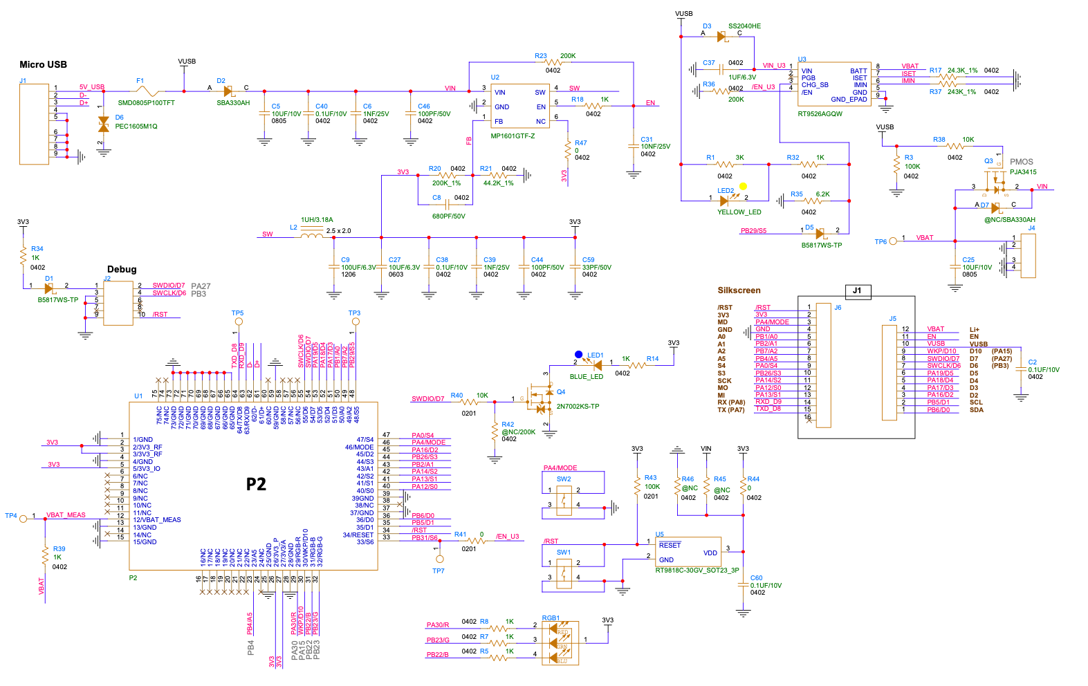
Schematic
Assembly
Water soluble flux
If you are attaching a Photon 2 to a custom base board, we recommend using a socket. As there are components on the bottom side of the Photon 2 there is no version available with castellated holes, solder pads, or similar techniques for direct surface mounting.
The pin headers on the bottom of the Photon 2 are not intended to be reflowed using paste-in-hole.
If you wish to surface mount module, you should directly use the P2 module on your base board instead of incorporating the Photon 2.
If you decide to wave solder or hand-solder the Photon 2 directly to your base board, water soluble flux should not be used. There are components within the P2 module that are moisture-sensitive, and wash water can get trapped under the RF shields, causing damage.
Use no-clean flux instead if you must solder the Photon 2 module.
Conformal coatings
Photon 2 modules should not use a conformal coating to protect the module from water. Some components on the module cannot be coated and would need to be masked off during coating. This will make the coating process difficult to implement and test.
Furthermore, the buttons cannot be protected by using a coating. Using an enclosure that protects both your base board and the Photon 2 module as a single waterproof assembly is recommended instead.
Ordering information
Photon 2 modules are available from store.particle.io.
| SKU | Description | Region | Lifecycle | Replacement |
|---|---|---|---|---|
| PHN2KIT | Photon 2, Kit [x1] | Global | GA | |
| PHN2MEA | Photon 2 [x1] | Global | GA | |
| PHN2MTY | Photon 2, Tray [x50] | Global | GA | |
| PHN2EDGEKIT | Edge ML Kit for Photon 2 (Photon 2 included) | Global | Deprecated |
Qualification and approvals

- RoHS
- CE
- FCC ID: 2AEMI-P2
- ISED: 20127-P2
Product handling
Moisture sensitivity levels
The Moisture Sensitivity Level (MSL) relates to the packaging and handling precautions required. The P1 module is rated level 3. In general, this precaution applies for Photons without headers. When reflowing a P1 directly onto an application PCB, increased moisture levels prior to reflow can damage sensitive electronics on the P1. A bake process to reduce moisture may be required.
For more information regarding moisture sensitivity levels, labeling, storage and drying see the MSL standard see IPC/JEDEC J-STD-020 (can be downloaded from www.jedec.org).
ESD precautions
The P1 module contains highly sensitive electronic circuitry and is an Electrostatic Sensitive Device (ESD). Handling a P1 module without proper ESD protection may destroy or damage it permanently. Proper ESD handling and packaging procedures must be applied throughout the processing, handling and operation of any application that incorporates P1 modules. ESD precautions should be implemented on the application board where the P1 module is mounted. Failure to observe these precautions can result in severe damage to the P1 module!
Default settings
The P2 module comes pre-programmed with a bootloader and a user application called Tinker. This application works with an iOS and Android app also named Tinker that allows you to very easily toggle digital pins, take analog and digital readings and drive variable PWM outputs.
The bootloader allows you to easily update the user application via several different methods, USB, OTA, Serial Y-Modem, and also internally via the Factory Reset procedure. All of these methods have multiple tools associated with them as well.
You may use the Particle Web IDE to code, compile and flash a user application OTA (Over The Air). Particle Workbench is a full-featured desktop IDE for Windows, Mac, and Linux based on VSCode and supports both cloud-based and local gcc-arm compiles. The Particle CLI provides a command-line interface for cloud-based compiles and flashing code over USB.
Glossary
FCC ISED CE warnings and end product labeling requirements
Federal Communication Commission Interference Statement
This equipment has been tested and found to comply with the limits for a Class B digital device, pursuant to Part 15 of the FCC Rules. These limits are designed to provide reasonable protection against harmful interference in a residential installation. This equipment generates, uses and can radiate radio frequency energy and, if not installed and used in accordance with the instructions, may cause harmful interference to radio communications. However, there is no guarantee that interference will not occur in a particular installation. If this equipment does cause harmful interference to radio or television reception, which can be determined by turning the equipment off and on, the user is encouraged to try to correct the interference by one of the following measures:
- Reorient or relocate the receiving antenna.
- Increase the separation between the equipment and receiver.
- Connect the equipment into an outlet on a circuit different from that to which the receiver is connected.
- Consult the dealer or an experienced radio/TV technician for help.
FCC Caution: Any changes or modifications not expressly approved by the party responsible for compliance could void the user's authority to operate this equipment. This device complies with Part 15 of the FCC Rules. Operation is subject to the following two conditions:
- This device may not cause harmful interference, and
- This device must accept any interference received, including interference that may cause undesired operation.
FCC Radiation Exposure Statement: This equipment complies with FCC radiation exposure limits set forth for an uncontrolled environment. This transmitter module must not be co-located or operating in conjunction with any other antenna or transmitter. This End equipment should be installed and operated with a minimum distance of 20 centimeters between the radiator and your body.
IMPORTANT NOTE: In the event that these conditions can not be met (for example certain laptop configurations or co-location with another transmitter), then the FCC authorization is no longer considered valid and the FCC ID can not be used on the final product. In these circumstances, the OEM integrator will be responsible for re-evaluating the end product (including the transmitter) and obtaining a separate FCC authorization.
End Product Labeling The final end product must be labeled in a visible area with the following:
Contains FCC ID: 2AEMI-P2
Manual Information to the End User The OEM integrator has to be aware not to provide information to the end user regarding how to install or remove this RF module in the user’s manual of the end product which integrates this module.
Outdoor Use (US)
To be compliant to FCC §15.407(a) the EIRP is not allowed to exceed 125 mW (21 dBm) at any elevation angle above 30° (measured from the horizon) when operated as an outdoor access point in U-NII-1 band, 5.150-5.250 GHz.
Canada Statement
This device complies with Industry Canada’s licence-exempt RSSs. Operation is subject to the following two conditions:
- This device may not cause interference; and
- This device must accept any interference, including interference that may cause undesired operation of the device.
Le présent appareil est conforme aux CNR d’Industrie Canada applicables aux appareils radio exempts de licence.
L’exploitation est autorisée aux deux conditions suivantes:
- l’appareil ne doit pas produire de brouillage;
- l’utilisateur de l’appareil doit accepter tout brouillage radioélectrique subi, même si le brouillage est susceptible d’en compromettre le fonctionnement.
Caution Exposure: This device meets the exemption from the routine evaluation limits in section 2.5 of RSS102 and users can obtain Canadian information on RF exposure and compliance. Le dispositif répond à l'exemption des limites d'évaluation de routine dans la section 2.5 de RSS102 et les utilisateurs peuvent obtenir des renseignements canadiens sur l'exposition aux RF et le respect.
The final end product must be labelled in a visible area with the following: The Industry Canada certification label of a module shall be clearly visible at all times when installed in the host device, otherwise the host device must be labelled to display the Industry Canada certification number of the module, preceded by the words “Contains transmitter module”, or the word “Contains”, or similar wording expressing the same meaning, as follows:
Contains transmitter module ISED: 20127-P2
This End equipment should be installed and operated with a minimum distance of 20 centimeters between the radiator and your body. Cet équipement devrait être installé et actionné avec une distance minimum de 20 centimètres entre le radiateur et votre corps.
The end user manual shall include all required regulatory information/warning as shown in this manual.
Restrictions of use
The products are used in terminal products such as industrial control equipment and smart home equipment.
Outdoor use (CA)
- Operation in the band 5150–5250 MHz is only for indoor use to reduce the potential for harmful interference to co-channel mobile satellite systems;
- Operation in the 5600-5650 MHz band is not allowed in Canada. High-power radars are allocated as primary users (i.e., priority users) of the bands 5250-5350 MHz and 5650-5850 MHz and that these radars could cause interference and/or damage to LE-LAN devices.
- Le dispositif de fonctionnement dans la bande 5150-5250 MHz est réservé à une utilisation en intérieur pour réduire le risque d'interférences nuisibles à la co-canal systèmes mobiles par satellite
- Opération dans la bande 5600-5650 MHz n'est pas autorisée au Canada. Haute puissance radars sont désignés comme utilisateurs principaux (c.-àutilisateurs prioritaires) des bandes 5250-5350 MHz et 5650-5850 MHz et que ces radars pourraient causer des interférences et / ou des dommages à dispositifs LAN-EL.
Transmitter specifications
| Frequency Range | RF power rating/field strength | Antenna information | Emissions designator |
|---|---|---|---|
| 2412-2462 MHz | 0.376704W | PCB Antenna, 2.41 dBi | 17M9D1D |
| 2402-2480 MHz | 0.009354W | PCB Antenna, 2.41 dBi | 1M02F1D |
| 2402-2480 MHz | 0.008670W | PCB Antenna, 2.41 dBi | 2M06F1D |
| 5180-5240/5190-5230 MHz | 0.073282/0081283W | PCB Antenna, 1.28 dBi | 18M6D1D/38M2D1D |
| 5260-5320/5270-5310 MHz | 0.081658/0.077090W | PCB Antenna, 1.60 dBi | 18M9D1D/37M5D1D |
| 5500-5700/5510-5670 MHz | 0.097949/0.091833W | PCB Antenna, 1.74 dBi | 19M2D1D/38M0D1D |
| 5745-5825/5755-5795 MHz | 0.091411/0.090365W | PCB Antenna, 1.21 dBi | 19M6D1D/36M8D1D |
Outdoor use (world)
This device is restricted to indoor use when operating in the 5150 to 5350 MHz frequency range. This restriction applies in: AT, BE, BG, CH, CY, CZ, DE, DK, EE, EL, ES, FI, FR, HR, HU, IE, IS, IT, LI, LT, LU, LV, MT, NL, NO, PL, PT, RO, SE, SI, SK, TR, UA, UK(NI).
Certification documents
CE (Europe) - Photon 2
- EU Declaration of Conformity (updated 2026-05-18)
- Certificate of Conformity
- Attestation
- EN 300-328 Bluetooth LE Test Report
- EN 300-328 Wi-Fi Test Report
- EN 300-440 Wi-Fi 5 GHz Test Report
- EN 301-489 Test Report
- EN 301-893 Wi-Fi 5 GHz Test Report
- EN 301-893 Dynamic Frequency Selection DFS Test Report
- EN62311 Test Report
- EN62368 Test Report
- EN62479 Test Report
FCC (United States) - Photon 2
- FCC ID: 2AEMI-P2 (this is the same as the P2 because the Photon 2 includes the P2 module)
- FCC Grant of Equipment Authorization (DTS)
- FCC Grant of Equipment Authorization (NII)
- FCC 15.247 Bluetooth LE Test Report
- FCC 15.247 Wi-Fi Test Report
- FCC 15.407 Test Report
ISED (Canada) - Photon 2
- ISED: 20127-P2 (this is the same as the P2 because the Photon 2 includes the P2 module)
- Certificate of Conformity
- ISED RSS-247 BTLE Test Report
- ISED RSS-247 Wi-Fi 2.4 GHz Test Report
- ISED RSS-247 Wi-Fi 5 GHz Test Report
RoHS - Photon 2
UKCA (United Kingdom) - Photon 2
Trace antenna test report - Photon 2
Revision history
| Revision | Date | Author | Comments |
|---|---|---|---|
| pre | 2022-03-02 | RK | Pre-release initial version |
| 2022-03-14 | RK | Minor edits; no functional changes | |
| 2022-04-08 | RK | Added table comparing Photon 2 and P2 pins | |
| 2022-04-12 | RK | Added serial baud rates | |
| 2022-04-16 | RK | Major changes to pinmap to align with P2 | |
| 2022-05-04 | RK | USB connector is micro B, not USB C | |
| 2022-08-12 | RK | Added listing of pins used at boot | |
| 2022-08-12 | RK | Warning about BLE central mode not available | |
| 2022-09-04 | RK | BLE central mode available, added power consumption | |
| 2022-10-05 | RK | Added power consumption | |
| 2022-11-08 | RK | Added external antenna | |
| 2022-11-17 | RK | Pin D0 does not have PWM | |
| 2023-01-31 | RK | Add Device OS versions | |
| 2023-02-14 | RK | Updated Photon 2 graphic to fix pin labels | |
| 2023-03-06 | RK | SWDIO is D7 not D8 | |
| 2023-03-08 | RK | Main CPU (KM4) is M33, not M23 | |
| 2023-03-24 | RK | Added FCC and ISED IDs | |
| 2023-04-03 | RK | Fixed typo in FCC ID in one location, ISED restrictions | |
| 2023-04-05 | RK | Added Device OS 5.3.1 information for SPI and retained memory | |
| 2023-04-10 | RK | Outdoor use restrictions | |
| 2023-04-24 | RK | Document VBAT_MEAS and CHG | |
| 2023-04-28 | RK | Add conformal coating and flux notes | |
| 2023-05-05 | RK | Update available RAM | |
| 2023-05-08 | RK | Added VBAT_MEAS and CHG to block diagram | |
| 2023-05-18 | RK | Add warning that the Photon 2 cannot be powered by 3V3 | |
| 1 | 2023-06-20 | RK | Initial version |
| 2 | 2023-06-30 | RK | Updated power consumption |
| 3 | 2023-07-26 | RK | EN pin description listed wrong MCU |
| 4 | 2023-11-13 | RK | Add full pin details |
| 5 | 2023-12-19 | RK | Add schematic |
| 6 | 2024-02-20 | RK | Added pin drive strength |
| 7 | 2024-03-11 | RK | Update CHG documentation |
| 8 | 2024-03-11 | RK | Added boot mode pin warning to GPIO pin table |
| 9 | 2024-03-12 | RK | Fix location of VUSB diode in block diagram |
| 10 | 2024-03-15 | RK | Update VUSB diode and descriptive text for VUSB |
| 11 | 2024-03-15 | RK | The UART baud rate 2400, 4800, 380400, 460800 are supported but were not listed |
| 12 | 2024-04-18 | RK | Add PDM microphone |
| 13 | 2024-04-23 | RK | Added links to certification documents |
| 14 | 2024-04-25 | RK | Update retained memory description |
| 15 | 2024-04-25 | RK | Added I/O characteristics |
| 16 | 2024-10-02 | RK | Added warning to not use Argon (ANT-FLXV2) antenna |
Known errata
Contact
Web
https://www.particle.io
Community Forums
https://community.particle.io