
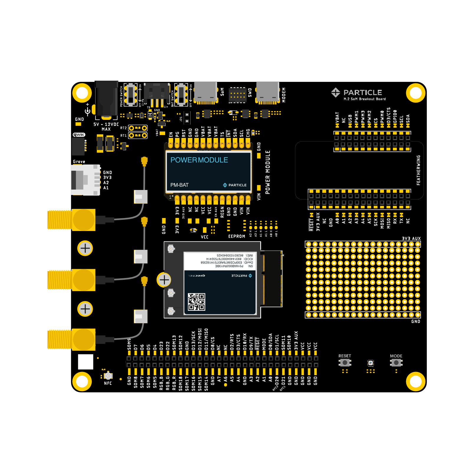
M.2 breakout board
The M.2 breakout board is a convenient way to prototype with the B-SoM and M-SoM modules.
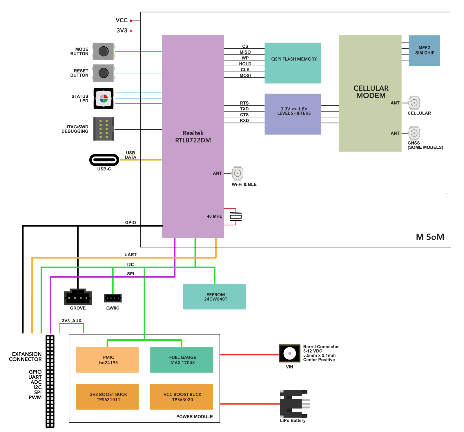
Block diagram
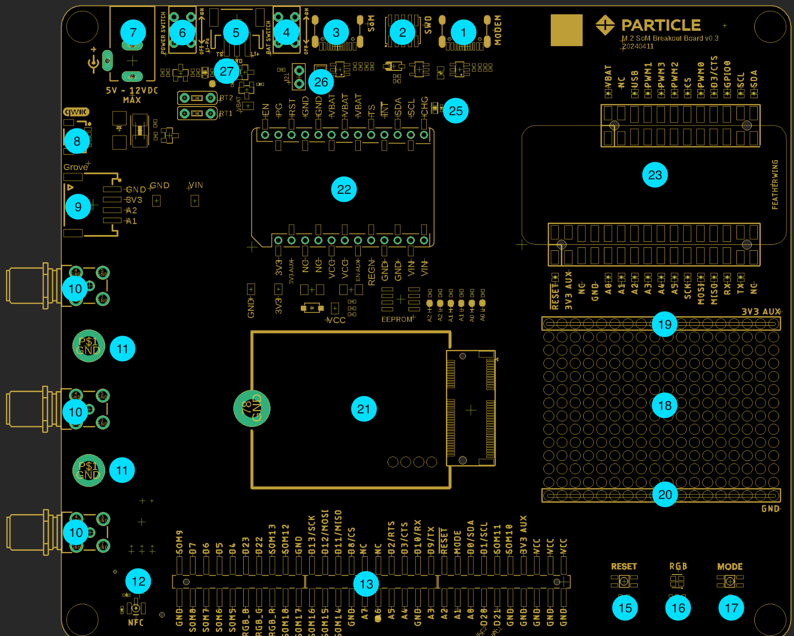
Board features
| Label | Description |
|---|---|
| 1 | Cellular modem USB-C (not normally used) |
| 2 | SWD debugging connector |
| 3 | MCU USB-C (use this one) |
| 4 | LiPo battery power switch |
| 5 | LiPo battery connector (3-pin, with temperature sensor) |
| 6 | DC power switch |
| 7 | DC power barrel connector (5.5mm x 2.1mm, center positive) |
| 8 | QWIIC (3.3V I2C connector) |
| 9 | Grove expansion connector |
| 10 | U.FL to SMA connectors |
| 11 | Spare M.2 SoM screws |
| 12 | NFC U.FL connector (B-SoM only, not available on M-SoM) |
| 13 | Expansion connector |
| 15 | RESET button |
| 16 | RGB status LED |
| 17 | MODE button |
| 18 | Prototyping area |
| 19 | 3V3_AUX |
| 20 | GND |
| 21 | M.2 SoM socket for B-SoM or M-SoM |
| 22 | Power module |
| 23 | Adafruit Feather connector (for accessories) |
| 25 | LiPo charge LED (yellow) |
| 26 | LiPo temperature sensor jumper (TS) |
| 27 | Power LED (red) |
Setup
Install the SoM
The M.2 SoM breakout board requires a Particle M-SoM or B-SoM module. Install it in the M.2 socket (21) and secure it with a thumbscrew.
Connect antennas
The M.2 breakout board can be used with the standard flexible Particle antennas or the SMA adapters included on the breakout board.
- Plug the cellular antenna into the U.FL connector labeled CELL on the SoM. Remember never to power up this board without the antenna being connected. There is potential to damage the transmitter of the u-blox module if no antenna is connected.
- If you are planning to use BLE, connect the 2.4 GHz antenna (the smaller one) to the BT U.FL connector on the SoM.
- The flexible Particle cellular and BLE antennas should be included in the M.2 SoM package, not the breakout board package.
- SMA antennas are not included with the M.2 breakout board. If used in a product, additional certification would be required to use a SMA antenna.
Install a power module
The M.2 breakout board includes two power modules; select and install the module you wish to use and install it in the power module socket (22).
Note the position of the notch to make sure the power module is installed in the correct orientation and make sure all of the pins are aligned with the socket on the breakout board.
PM-BAT power module
The PM-BAT power module allows the Particle SoM to be powered by a LiPo battery or DC adapter.
- Install the PM-BAT module in the power module socket (22).
- Connect the LiPo battery (2).
- Optionally connect the AC power adapter to VIN (7). With PM-BAT, VIN must be 5 - 12 VDC.
- You must use the LiPo battery, AC power adapter, or both, when using PM-BAT. You cannot power by USB only.
- The LiPo battery can be only be charged by VIN, it cannot be charged from USB.
PM-DC power module
The PM-DC power module allows the Particle SoM to be powered by an AC power adapter or external DC power source.
- Install the PM-DC module in the power module socket (22).
- Connect the power adapter to VIN (7). When powering PM-DC by VIN (barrel connector), 5 - 12 VDC is required at 12 watts.
- Power on the VIN barrel connector is required when using PM-DC; you cannot power the breakout board only by USB power.
Power on device
Turn on the appropriate power switches (4, 6).
The RGB status LED should turn on. Typically it will blink white once, then blink green though it may display a different pattern.
Device setup and claiming
Connect the USB connector (3) to your computer. This is needed only for setup.
Visit https://setup.particle.io/ to finish setting up your device.
Onboard peripherals
Qwiic (8)
The SparkFun Qwiic system provides an easy way to expand and test various sensors, input devices, and displays. Multiple peripherals can be daisy-chained to a single port. The Adafruit Stemma QT are compatible with Qwiic and can be mixed and matched as well.
For more information, see Qwiic.
Grove connector (9)
Additionally, Grove system of sensors and peripherals from Seeed Systems is another easy way to add peripheral devices. The M.2 breakout board has one Grove connectors connected to pins A1 and A2 that can be used as GPIO or analog inputs. This port cannot be used with I2C or Serial Grove peripherals.
| J11 | SoM Pin | SoM Pin Number |
|---|---|---|
| GND | ||
| 3V3 | ||
| ADC2 | A2 | 35 |
| ADC1 | A1 | 33 |
Feather connector (21)
The Feather connector can be used for Adafruit FeatherWings, such as displays, sensors, and Ethernet. You cannot plug a Feather MCU into this socket!
Feather pin mapping - M-SoM

Feather pin mapping - B-SoM

Jumpers (22)
These jumpers connect the Feather A pin side to the M.2 connector. They can also be used to remap pins by using jumper wires instead of solid jumpers.
Jumpers (23)
These jumpers connect the Feather D pin side to the M.2 connector. They can also be used to remap pins by using jumper wires instead of solid jumpers.
LiPo connector
Note that the M.2 breakout board includes a 3-pin JST-PH connector (left), not the 2-pin JST-PH connector on some other Particle devices (right). The TS pin is expected to be connected to a 10K NTC thermistor in the battery pack. The TS jumper (26) must be installed for normal operation with a temperature sensor.
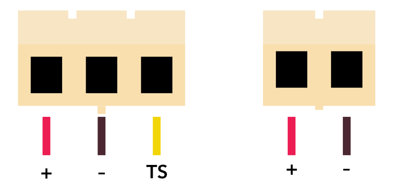
Looking at the exposed end of the connector attached to the battery
If you wish to use a battery without a temperature sensor, remove the TS jumper (26) and use a 3-pin to 2-pin JST-PH adapter, or change the shell of your JST-PH 2-pin connector to a 3-pin shell. The pin can be swapped without cutting, soldering, or crimping. See the battery guide for more information.
If purchasing a LiPo battery from a 3rd-party supplier, beware as the polarity of the JST-PH connector is not standardized and may be reversed. Permanent damage to the breakout board can occur if powered by reverse polarity on the JST connector. See the battery guide for additional information.
The included battery is a 3100 mAh 3.7V LiPo battery with temperature sensor. Battery datasheet.
3V3_AUX power
Both the PM-BAT and PM-DC power modules support an auxiliary 3.3V power supply. This is used to power the Feather socket 3V3 and the 3V3_AUX rail.
| Power module | SoM Pin | SoM Pin Number |
|---|---|---|
| EN_AUX | D23 / GPIO1 | 50 |
3V3_AUX is powered from 3V3 via a load switch (TPS22918). It can supply up to the full 2A of 3V3. It defaults to off due to a pull-down resistor on EN_AUX. EN_AUX is connected to pin D23; set this pin to output high to enable 3V3_AUX.
// Enable 3V3_AUX
pinMode(D23, OUTPUT);
digitalWrite(D23, HIGH);
Devices using the Particle Power Module include a 3V3_AUX power output
that can be controlled by a GPIO. On the M.2 SoM breakout board, this powers the Feather connector. On the Muon,
it powers the Ethernet port, LoRaWAN module, 40-pin expansion HAT connector, and QWIIC connector.
The main reason for this is that until the PMIC is configured, the input current with no battery
connected is limited to 100 mA. This is insufficient for the M-SoM to boot when
using a peripheral that requires a lot of current, like the WIZnet W5500 Ethernet module. The
system power manager prevents turning on 3V3_AUX until after the PMIC is configured
and the PMIC has negotiated a higher current from the USB host (if powered by USB).
This setting is persistent and only needs to be set once. In fact, the PMIC initialization
normally occurs before user firmware is run. This is also necessary because if you are using Ethernet
and enter safe mode (breathing magenta), it's necessary to enable 3V3_AUX so if you are using
Ethernet, you can still get OTA updates while in safe mode.
After changing the auxiliary power configuration you must reset the device.
PM-BAT interface
The M.2 breakout board can be used with the PM-BAT power module that includes the bq24195 PMIC and MAX17043 fuel gauge chips which interface by the pins below
| Power module | SoM Pin | SoM Pin Number |
|---|---|---|
| FUEL_INT | A6 | 45 |
| SDA | D0 | 22 |
| SCL | D1 | 20 |
Using ethernet
The M.2 breakout board does not contain Ethernet like the previous B-Series Eval board. You can, however, add it using the Adafruit Ethernet FeatherWing in the Feather socket.
Be sure to connect the nRESET and nINTERRUPT pins (on the small header on the short side) to pins D3 and D4 with jumper wires. These are required for proper operation.
The default mapping for the B-SoM and the original B-SoM eval board is listed below, but you may want to use Ethernet pin remapping to reassign the pins.
| Particle Pin | M.2 Pin | Ethernet Pin |
|---|---|---|
| D8 | CS | ETH_CS |
| A7 | RESERVED | ETH_RESET |
| SCK | SCK | ETH_CLK |
| MISO | MISO | ETH_MISO |
| MOSI | MOSI | ETH_MOSI |
| D22 | GPIO0 | ETH_INT |
Firmware example
The following code can be used to enable Ethernet on the M.2 SoM breakout board. This only needs to be done once and the device must be reset after configuration for the changes to take effect. It requires Device OS 5.9.0 or later.
// Enable 3V3_AUX
SystemPowerConfiguration powerConfig = System.getPowerConfiguration();
powerConfig.auxiliaryPowerControlPin(D23).interruptPin(A6);
System.setPowerConfiguration(powerConfig);

// Enable Ethernet
if_wiznet_pin_remap remap = {};
remap.base.type = IF_WIZNET_DRIVER_SPECIFIC_PIN_REMAP;

System.enableFeature(FEATURE_ETHERNET_DETECTION);
remap.cs_pin = D5;
remap.reset_pin = PIN_INVALID;
remap.int_pin = PIN_INVALID;
auto ret = if_request(nullptr, IF_REQ_DRIVER_SPECIFIC, &remap, sizeof(remap), nullptr);
Using SD card
The M.2 breakout board does not contain a Micro SD card socket as the previous B-Series Eval board did. You can, however, add it using the Adafruit Feather connector.
The Adalogger FeatherWing - RTC + SD Add-on For All Feather Boards contains a Micro SD card socket.
| SD Card Pin | Feather Pin | Description |
|---|---|---|
| SCK | SCK | SPI Clock |
| MOSI | MOSI | Data (MCU to SD card) |
| MISO | MISO | Data (SD card to MCU) |
| SDCS | D5 | Chip select |
It is also possible to cut the a trace jumper for SDCS and use a different pin for SDCS. Note that this will use SPI (primary SPI) but the B-Series Eval board use SPI1 so your SD card initialization code will be different.
See the Adafruit tutorial for additional information.
Expansion header
Expansion header - M-SoM

Expansion header - B-SoM

Full pin listing
Skip past this section (the full pin listing is long)
Module Pin 1 (GND)
| Unchanged between B-SoM and M-SoM | |
|---|---|
| Pin Number | 1 |
| Pin Name | GND |
| Description | Ground. |
| M.2 connector pin number | 1 |
| SoM Common Pin Name | GND |
Module Pin 2 (VCC)
| Unchanged between B-SoM and M-SoM | |
|---|---|
| Pin Number | 2 |
| Pin Name | VCC |
| Description | Cellular modem power. Typically 3.9V, can be 3.6V to 4.2V |
| M.2 connector pin number | 2 |
| SoM Common Pin Name | VCC |
Module Pin 3 (GND)
| Unchanged between B-SoM and M-SoM | |
|---|---|
| Pin Number | 3 |
| Pin Name | GND |
| Description | Ground. |
| M.2 connector pin number | 1 |
| SoM Common Pin Name | GND |
Module Pin 4 (VCC)
| Unchanged between B-SoM and M-SoM | |
|---|---|
| Pin Number | 4 |
| Pin Name | VCC |
| Description | Cellular modem power. Typically 3.9V, can be 3.6V to 4.2V |
| M.2 connector pin number | 2 |
| SoM Common Pin Name | VCC |
Module Pin 5 (GND)
| Unchanged between B-SoM and M-SoM | |
|---|---|
| Pin Number | 5 |
| Pin Name | GND |
| Description | Ground. |
| M.2 connector pin number | 1 |
| SoM Common Pin Name | GND |
Module Pin 6 (VCC)
| Unchanged between B-SoM and M-SoM | |
|---|---|
| Pin Number | 6 |
| Pin Name | VCC |
| Description | Cellular modem power. Typically 3.9V, can be 3.6V to 4.2V |
| M.2 connector pin number | 2 |
| SoM Common Pin Name | VCC |
Module Pin 7 (GND)
| Unchanged between B-SoM and M-SoM | |
|---|---|
| Pin Number | 7 |
| Pin Name | GND |
| Description | Ground. |
| M.2 connector pin number | 1 |
| SoM Common Pin Name | GND |
Module Pin 8 (3V3)
| B-SoM | M-SoM | ||
|---|---|---|---|
| Pin Number | 8 | 8 | |
| Pin Name | 3V3 | 3V3 | |
| Description | 3.3V used to power MCU | 3.3V used to power MCU | |
| ∆ | M.2 connector pin number | 10 | 8 |
| ∆ | SoM Common Pin Name | 3V3 | VCC |
Module Pin 9 (GND)
| Unchanged between B-SoM and M-SoM | |
|---|---|
| Pin Number | 9 |
| Pin Name | GND |
| Description | Ground. |
| M.2 connector pin number | 1 |
| SoM Common Pin Name | GND |
Module Pin 10 (SOM10)
| Unchanged between B-SoM and M-SoM | |
|---|---|
| Pin Number | 10 |
| Pin Name | SOM10 |
| Description | Not currently used, leave unconnected. |
| M.2 connector pin number | 14 |
| SoM Common Pin Name | RESERVED |
Module Pin 11 (SOM6 / D21)
| B-SoM | M-SoM | ||
|---|---|---|---|
| Pin Number | 11 | 11 | |
| ∆ | Pin Name | SOM6 | D21 |
| ∆ | Pin Alternate Name | NFC1 | n/a |
| ∆ | Description | NFC Antenna 1. | D21 GPIO. Is NFC1 on B-SoM. |
| ∆ | Supports digitalRead | n/a | Yes |
| ∆ | Supports digitalWrite | n/a | Yes |
| ∆ | Supports attachInterrupt | n/a | Yes |
| ∆ | I2S interface | n/a | I2S RX |
| ∆ | Internal pull resistance | n/a | 22K. No internal pull up or pull down in HIBERNATE sleep mode. |
| M.2 connector pin number | 17 | 17 | |
| ∆ | SoM Common Pin Name | SOM3 | RESERVED |
Module Pin 12 (SOM11 / GNSS_TX)
| B-SoM | M-SoM | ||
|---|---|---|---|
| Pin Number | 12 | 12 | |
| ∆ | Pin Name | SOM11 | GNSS_TX |
| ∆ | Description | Not currently used, leave unconnected. | Cellular modem GNSS UART TX |
| M.2 connector pin number | 18 | 18 | |
| SoM Common Pin Name | RESERVED | RESERVED |
Module Pin 13 (SOM7 / D20)
| B-SoM | M-SoM | ||
|---|---|---|---|
| Pin Number | 13 | 13 | |
| ∆ | Pin Name | SOM7 | D20 |
| ∆ | Pin Alternate Name | NFC2 | n/a |
| ∆ | Description | NFC Antenna 2. NFC2 is the center pin. | D20 GPIO. Is NFC2 on B-SoM. |
| ∆ | Supports digitalRead | n/a | Yes |
| ∆ | Supports digitalWrite | n/a | Yes |
| ∆ | Supports attachInterrupt | n/a | Yes |
| ∆ | I2S interface | n/a | I2S TX |
| ∆ | Internal pull resistance | n/a | ??? |
| M.2 connector pin number | 19 | 19 | |
| ∆ | SoM Common Pin Name | SOM4 | RESERVED |
Module Pin 14 (D1)
| B-SoM | M-SoM | ||
|---|---|---|---|
| Pin Number | 14 | 14 | |
| Pin Name | D1 | D1 | |
| Pin Alternate Name | D1 | D1 | |
| Description | I2C SCL. Cannot be used as GPIO. | I2C SCL. Cannot be used as GPIO. | |
| Supports digitalRead | Yes | Yes | |
| Supports digitalWrite | Yes | Yes | |
| ∆ | I2C interface | SCL. Use Wire object. | SCL. Use Wire object. Use 1.5K to 10K external pull-up resistor. |
| ∆ | Supports attachInterrupt | Yes. You can only have 8 active interrupt pins. | Yes |
| ∆ | Internal pull resistance | 13K | ??? |
| M.2 connector pin number | 20 | 20 | |
| SoM Common Pin Name | SCL | SCL |
Module Pin 15 (A0)
| B-SoM | M-SoM | ||
|---|---|---|---|
| Pin Number | 15 | 15 | |
| Pin Name | A0 | A0 | |
| Pin Alternate Name | D19 | D19 | |
| Description | A0 Analog in, GPIO, PWM | A0 Analog in, GPIO, PWM | |
| Supports digitalRead | Yes | Yes | |
| Supports digitalWrite | Yes | Yes | |
| Supports analogRead | Yes | Yes | |
| Supports analogWrite (PWM) | Yes | Yes | |
| ∆ | Supports tone | A0, A1, A6, and A7 must have the same frequency. | Yes |
| ∆ | Supports attachInterrupt | Yes. You can only have 8 active interrupt pins. | Yes |
| ∆ | Internal pull resistance | 13K | 42K |
| M.2 connector pin number | 23 | 23 | |
| SoM Common Pin Name | ADC0 | ADC0 |
Module Pin 16 (D0)
| B-SoM | M-SoM | ||
|---|---|---|---|
| Pin Number | 16 | 16 | |
| Pin Name | D0 | D0 | |
| Pin Alternate Name | D0 | D0 | |
| Description | I2C SDA. Cannot be used as GPIO. | I2C SDA. Cannot be used as GPIO. | |
| Supports digitalRead | Yes | Yes | |
| Supports digitalWrite | Yes | Yes | |
| ∆ | I2C interface | SDA. Use Wire object. | SDA. Use Wire object. Use 1.5K to 10K external pull-up resistor. |
| ∆ | Supports attachInterrupt | Yes. You can only have 8 active interrupt pins. | Yes |
| ∆ | Internal pull resistance | 13K | ??? |
| M.2 connector pin number | 22 | 22 | |
| SoM Common Pin Name | SDA | SDA |
Module Pin 17 (A1)
| B-SoM | M-SoM | ||
|---|---|---|---|
| Pin Number | 17 | 17 | |
| Pin Name | A1 | A1 | |
| Pin Alternate Name | D18 | D18 | |
| Description | A1 Analog in, GPIO, PWM | A1 Analog in, GPIO, PWM | |
| Supports digitalRead | Yes | Yes | |
| Supports digitalWrite | Yes | Yes | |
| Supports analogRead | Yes | Yes | |
| Supports analogWrite (PWM) | Yes | Yes | |
| ∆ | Supports tone | A0, A1, A6, and A7 must have the same frequency. | Yes |
| ∆ | Supports attachInterrupt | Yes. You can only have 8 active interrupt pins. | Yes |
| ∆ | Internal pull resistance | 13K | ??? |
| M.2 connector pin number | 33 | 33 | |
| SoM Common Pin Name | ADC1 | ADC1 |
Module Pin 18 (MODE)
| B-SoM | M-SoM | ||
|---|---|---|---|
| Pin Number | 18 | 18 | |
| Pin Name | MODE | MODE | |
| Pin Alternate Name | D20 | D20 | |
| ∆ | Description | MODE button, has internal pull-up | MODE button. Pin number constant is BTN. External pull-up required! |
| ∆ | Supports attachInterrupt | n/a | Yes |
| M.2 connector pin number | 32 | 32 | |
| SoM Common Pin Name | MODE | MODE |
Module Pin 19 (A2)
| B-SoM | M-SoM | ||
|---|---|---|---|
| Pin Number | 19 | 19 | |
| Pin Name | A2 | A2 | |
| Pin Alternate Name | D17 | D17 | |
| Description | A2 Analog in, GPIO | A2 Analog in, GPIO | |
| Supports digitalRead | Yes | Yes | |
| Supports digitalWrite | Yes | Yes | |
| Supports analogRead | Yes | Yes | |
| ∆ | Supports attachInterrupt | Yes. You can only have 8 active interrupt pins. | Yes |
| ∆ | Internal pull resistance | 13K | 22K |
| M.2 connector pin number | 35 | 35 | |
| SoM Common Pin Name | ADC2 | ADC2 |
Module Pin 20 (RST)
| B-SoM | M-SoM | ||
|---|---|---|---|
| Pin Number | 20 | 20 | |
| Pin Name | RST | RST | |
| ∆ | Description | Hardware reset, active low. | Hardware reset, active low. External pull-up required. |
| M.2 connector pin number | 34 | 34 | |
| SoM Common Pin Name | RESET | RESET |
Module Pin 21 (A3)
| B-SoM | M-SoM | ||
|---|---|---|---|
| Pin Number | 21 | 21 | |
| Pin Name | A3 | A3 | |
| Pin Alternate Name | D16 | D16 | |
| ∆ | Description | A3 Analog in, GPIO | A3 Analog in, PDM CLK, GPIO |
| Supports digitalRead | Yes | Yes | |
| Supports digitalWrite | Yes | Yes | |
| Supports analogRead | Yes | Yes | |
| ∆ | Supports attachInterrupt | Yes. You can only have 8 active interrupt pins. | Yes |
| ∆ | Internal pull resistance | 13K | 2.1K |
| M.2 connector pin number | 37 | 37 | |
| SoM Common Pin Name | ADC3 | ADC3 |
Module Pin 22 (TX)
| B-SoM | M-SoM | ||
|---|---|---|---|
| Pin Number | 22 | 22 | |
| Pin Name | TX | TX | |
| Pin Alternate Name | D9 | D9 | |
| ∆ | Description | Serial TX, GPIO | Serial TX, PWM, GPIO, SPI1 MOSI |
| Supports digitalRead | Yes | Yes | |
| Supports digitalWrite | Yes | Yes | |
| ∆ | Supports analogWrite (PWM) | No | Yes |
| ∆ | Supports tone | No | Yes |
| UART serial | TX. Use Serial1 object. | TX. Use Serial1 object. | |
| ∆ | SPI interface | n/a | MOSI. Use SPI1 object. |
| ∆ | Supports attachInterrupt | Yes. You can only have 8 active interrupt pins. | Yes |
| ∆ | I2S interface | n/a | I2S MCLK |
| ∆ | Internal pull resistance | 13K | 2.1K |
| M.2 connector pin number | 36 | 36 | |
| SoM Common Pin Name | TX | TX |
Module Pin 23 (GND)
| Unchanged between B-SoM and M-SoM | |
|---|---|
| Pin Number | 23 |
| Pin Name | GND |
| Description | Ground. |
| M.2 connector pin number | 1 |
| SoM Common Pin Name | GND |
Module Pin 24 (RX)
| B-SoM | M-SoM | ||
|---|---|---|---|
| Pin Number | 24 | 24 | |
| Pin Name | RX | RX | |
| Pin Alternate Name | D10 | D10 | |
| ∆ | Description | Serial RX, GPIO | Serial RX, PWM, GPIO, SPI1 MISO |
| Supports digitalRead | Yes | Yes | |
| Supports digitalWrite | Yes | Yes | |
| ∆ | Supports analogWrite (PWM) | No | Yes |
| ∆ | Supports tone | No | Yes |
| UART serial | RX. Use Serial1 object. | RX. Use Serial1 object. | |
| ∆ | SPI interface | n/a | MISO. Use SPI1 object. |
| ∆ | Supports attachInterrupt | Yes. You can only have 8 active interrupt pins. | Yes |
| ∆ | Internal pull resistance | 13K | 2.1K |
| M.2 connector pin number | 38 | 38 | |
| SoM Common Pin Name | RX | RX |
Module Pin 25 (A4)
| B-SoM | M-SoM | ||
|---|---|---|---|
| Pin Number | 25 | 25 | |
| Pin Name | A4 | A4 | |
| Pin Alternate Name | D15 | D15 | |
| ∆ | Description | A4 Analog in, GPIO | A4 Analog in, PDM DAT, GPIO |
| Supports digitalRead | Yes | Yes | |
| Supports digitalWrite | Yes | Yes | |
| Supports analogRead | Yes | Yes | |
| ∆ | Supports attachInterrupt | Yes. You can only have 8 active interrupt pins. | Yes |
| ∆ | Internal pull resistance | 13K | 2.1K |
| M.2 connector pin number | 41 | 41 | |
| SoM Common Pin Name | RESERVED | RESERVED |
Module Pin 26 (D3)
| B-SoM | M-SoM | ||
|---|---|---|---|
| Pin Number | 26 | 26 | |
| Pin Name | D3 | D3 | |
| Pin Alternate Name | CTS | CTS | |
| ∆ | Description | SPI1 MOSI, Serial1 CTS, GPIO, Wire1 SCL | D3 GPIO, Serial1 CTS flow control (optional), SPI1 SS |
| Supports digitalRead | Yes | Yes | |
| Supports digitalWrite | Yes | Yes | |
| UART serial | CTS. Use Serial1 object. | CTS. Use Serial1 object. | |
| ∆ | SPI interface | MOSI. Use SPI1 object. | SS. Use SPI1 object. |
| I2C interface | SCL. Use Wire1 object. | SCL. Use Wire1 object. | |
| ∆ | Supports attachInterrupt | Yes. You can only have 8 active interrupt pins. | Yes |
| ∆ | Internal pull resistance | 13K | ??? |
| M.2 connector pin number | 40 | 40 | |
| ∆ | SoM Common Pin Name | RESERVED | CTS |
Module Pin 27 (A5)
| B-SoM | M-SoM | ||
|---|---|---|---|
| Pin Number | 27 | 27 | |
| Pin Name | A5 | A5 | |
| Pin Alternate Name | D14 | D14 | |
| ∆ | Description | A5 Analog in, GPIO | A5 Analog in, PWM, GPIO, shared with pin 53 |
| Supports digitalRead | Yes | Yes | |
| Supports digitalWrite | Yes | Yes | |
| Supports analogRead | Yes | Yes | |
| ∆ | Supports analogWrite (PWM) | No | Yes |
| ∆ | Supports tone | No | Yes |
| ∆ | Supports attachInterrupt | Yes. You can only have 8 active interrupt pins. | Yes |
| ∆ | Internal pull resistance | 13K | ??? |
| ∆ | SWD interface | n/a | SWCLK. 40K pull-down at boot. |
| ∆ | Signal used at boot | n/a | SWCLK. 40K pull-down at boot. |
| M.2 connector pin number | 43 | 43 | |
| SoM Common Pin Name | RESERVED | RESERVED |
Module Pin 28 (D2)
| B-SoM | M-SoM | ||
|---|---|---|---|
| Pin Number | 28 | 28 | |
| Pin Name | D2 | D2 | |
| Pin Alternate Name | RTS | RTS | |
| ∆ | Description | SPI1 SCK, Serial1 RTS, PWM, GPIO, Wire1 SDA | D2 GPIO, Serial RTS flow control (optional), SPI1 SCK |
| Supports digitalRead | Yes | Yes | |
| Supports digitalWrite | Yes | Yes | |
| UART serial | RTS. Use Serial1 object. | RTS. Use Serial1 object. | |
| SPI interface | SCK. Use SPI1 object. | SCK. Use SPI1 object. | |
| I2C interface | SDA. Use Wire1 object. | SDA. Use Wire1 object. | |
| ∆ | Supports attachInterrupt | Yes. You can only have 8 active interrupt pins. | Yes |
| ∆ | Internal pull resistance | 13K | ??? |
| M.2 connector pin number | 42 | 42 | |
| ∆ | SoM Common Pin Name | RESERVED | RTS |
Module Pin 29 (A6)
| B-SoM | M-SoM | ||
|---|---|---|---|
| Pin Number | 29 | 29 | |
| Pin Name | A6 | A6 | |
| ∆ | Pin Alternate Name | D16 | D29 |
| ∆ | Description | A6 Analog in, PWM, GPIO | A6 Analog in, GPIO, PWM, M.2 eval PMIC INT |
| Supports digitalRead | Yes | Yes | |
| Supports digitalWrite | Yes | Yes | |
| Supports analogRead | Yes | Yes | |
| Supports analogWrite (PWM) | Yes | Yes | |
| ∆ | Supports tone | A0, A1, A6, and A7 must have the same frequency. | Yes |
| ∆ | Supports attachInterrupt | Yes. You can only have 8 active interrupt pins. | Yes |
| ∆ | Internal pull resistance | 13K | ??? |
| M.2 connector pin number | 45 | 45 | |
| SoM Common Pin Name | RESERVED | RESERVED |
Module Pin 30 (SOM0 / CELL USBD+)
| B-SoM | M-SoM | ||
|---|---|---|---|
| Pin Number | 30 | 30 | |
| ∆ | Pin Name | SOM0 | CELL USBD+ |
| Pin Alternate Name | CELL USBD+ | CELL USBD+ | |
| ∆ | Description | Cellular Modem USB Data+. | Cellular Modem USB Data+ |
| Input is 5V Tolerant | Yes | Yes | |
| M.2 connector pin number | 44 | 44 | |
| SoM Common Pin Name | SOM0 | SOM0 |
Module Pin 31 (A7)
| B-SoM | M-SoM | ||
|---|---|---|---|
| Pin Number | 31 | 31 | |
| Pin Name | A7 | A7 | |
| ∆ | Pin Alternate Name | D17 | WKP |
| ∆ | Description | A7 Analog in, GPIO | A7 Analog In, WKP, GPIO D28 |
| Supports digitalRead | Yes | Yes | |
| Supports digitalWrite | Yes | Yes | |
| Supports analogRead | Yes | Yes | |
| ∆ | Supports analogWrite (PWM) | Yes | No |
| ∆ | Supports tone | A0, A1, A6, and A7 must have the same frequency. | No |
| ∆ | Supports attachInterrupt | Yes. You can only have 8 active interrupt pins. | Yes |
| ∆ | Internal pull resistance | 13K | ??? |
| M.2 connector pin number | 47 | 47 | |
| SoM Common Pin Name | RESERVED | RESERVED |
Module Pin 32 (SOM1 / CELL USBD-)
| B-SoM | M-SoM | ||
|---|---|---|---|
| Pin Number | 32 | 32 | |
| ∆ | Pin Name | SOM1 | CELL USBD- |
| Pin Alternate Name | CELL USBD- | CELL USBD- | |
| ∆ | Description | Cellular Modem USB Data-. | Cellular Modem USB Data- |
| Input is 5V Tolerant | Yes | Yes | |
| M.2 connector pin number | 46 | 46 | |
| SoM Common Pin Name | SOM1 | SOM1 |
Module Pin 33 (GND)
| Unchanged between B-SoM and M-SoM | |
|---|---|
| Pin Number | 33 |
| Pin Name | GND |
| Description | Ground. |
| M.2 connector pin number | 1 |
| SoM Common Pin Name | GND |
Module Pin 34 (D8)
| B-SoM | M-SoM | ||
|---|---|---|---|
| Pin Number | 34 | 34 | |
| Pin Name | D8 | D8 | |
| ∆ | Pin Alternate Name | CS | D8 |
| ∆ | Description | GPIO, SPI SS | D8 GPIO, SPI SS |
| Supports digitalRead | Yes | Yes | |
| Supports digitalWrite | Yes | Yes | |
| ∆ | SPI interface | SS. Use SPI object. This is only the default SS/CS pin, you can use any GPIO instead. | Default SS for SPI. |
| ∆ | Supports attachInterrupt | Yes. You can only have 8 active interrupt pins. | Yes |
| ∆ | Internal pull resistance | 13K | 2.1K |
| M.2 connector pin number | 48 | 48 | |
| SoM Common Pin Name | CS | CS |
Module Pin 35 (SOM14)
| Unchanged between B-SoM and M-SoM | |
|---|---|
| Pin Number | 35 |
| Pin Name | SOM14 |
| Description | M.2 pin 51. Not currently used, leave unconnected. |
| M.2 connector pin number | 51 |
| SoM Common Pin Name | RESERVED |
Module Pin 36 (MISO)
| B-SoM | M-SoM | ||
|---|---|---|---|
| Pin Number | 36 | 36 | |
| Pin Name | MISO | MISO | |
| Pin Alternate Name | D11 | D11 | |
| ∆ | Description | SPI MISO, GPIO | D11 GPIO, PWM, SPI MISO |
| Supports digitalRead | Yes | Yes | |
| Supports digitalWrite | Yes | Yes | |
| ∆ | Supports analogWrite (PWM) | No | Yes |
| ∆ | Supports tone | No | Yes |
| SPI interface | MISO. Use SPI object. | MISO. Use SPI object. | |
| ∆ | Supports attachInterrupt | Yes. You can only have 8 active interrupt pins. | Yes |
| ∆ | Internal pull resistance | 13K | 2.1K |
| M.2 connector pin number | 50 | 50 | |
| SoM Common Pin Name | MISO | MISO |
Module Pin 37 (SOM15 / A5)
| B-SoM | M-SoM | ||
|---|---|---|---|
| Pin Number | 37 | 37 | |
| ∆ | Pin Name | SOM15 | A5 |
| ∆ | Pin Alternate Name | n/a | D14 |
| ∆ | Description | M.2 pin 53. Not currently used, leave unconnected. | A5 Analog in, PWM, GPIO, SWCLK, shared with pin 43 |
| ∆ | Supports digitalRead | n/a | Yes |
| ∆ | Supports digitalWrite | n/a | Yes |
| ∆ | Supports analogRead | n/a | Yes |
| ∆ | Supports analogWrite (PWM) | n/a | Yes |
| ∆ | Supports tone | n/a | Yes |
| ∆ | Supports attachInterrupt | n/a | Yes |
| ∆ | Internal pull resistance | n/a | 42K |
| ∆ | SWD interface | n/a | SWCLK. 40K pull-down at boot. |
| ∆ | Signal used at boot | n/a | SWCLK. 40K pull-down at boot. |
| M.2 connector pin number | 53 | 53 | |
| ∆ | SoM Common Pin Name | RESERVED | SWD_CLK |
Module Pin 38 (MOSI)
| B-SoM | M-SoM | ||
|---|---|---|---|
| Pin Number | 38 | 38 | |
| Pin Name | MOSI | MOSI | |
| Pin Alternate Name | D12 | D12 | |
| ∆ | Description | SPI MOSI, GPIO | D12 GPIO, PWM, SPI MOSI |
| Supports digitalRead | Yes | Yes | |
| Supports digitalWrite | Yes | Yes | |
| ∆ | Supports analogWrite (PWM) | No | Yes |
| ∆ | Supports tone | No | Yes |
| SPI interface | MOSI. Use SPI object. | MOSI. Use SPI object. | |
| ∆ | Supports attachInterrupt | Yes. You can only have 8 active interrupt pins. | Yes |
| ∆ | Internal pull resistance | 13K | 2.1K |
| M.2 connector pin number | 52 | 52 | |
| SoM Common Pin Name | MOSI | MOSI |
Module Pin 39 (SOM16 / D27)
| B-SoM | M-SoM | ||
|---|---|---|---|
| Pin Number | 39 | 39 | |
| ∆ | Pin Name | SOM16 | D27 |
| ∆ | Description | M.2 pin 55. Not currently used, leave unconnected. | D27 GPIO, SWDIO (SWD_DATA), do not pull down at boot |
| ∆ | Supports digitalRead | n/a | Yes |
| ∆ | Supports digitalWrite | n/a | Yes |
| ∆ | Supports attachInterrupt | n/a | Yes |
| ∆ | Internal pull resistance | n/a | 42K |
| ∆ | SWD interface | n/a | SWDIO. 40K pull-up at boot. |
| ∆ | Signal used at boot | n/a | SWDIO. 40K pull-up at boot. Low at boot triggers MCU test mode. |
| M.2 connector pin number | 55 | 55 | |
| ∆ | SoM Common Pin Name | RESERVED | SWD_DATA |
Module Pin 40 (SCK)
| B-SoM | M-SoM | ||
|---|---|---|---|
| Pin Number | 40 | 40 | |
| Pin Name | SCK | SCK | |
| Pin Alternate Name | D13 | D13 | |
| ∆ | Description | SPI SCK, GPIO | D13 GPIO, SPI SCK |
| Supports digitalRead | Yes | Yes | |
| Supports digitalWrite | Yes | Yes | |
| SPI interface | SCK. Use SPI object. | SCK. Use SPI object. | |
| ∆ | Supports attachInterrupt | Yes. You can only have 8 active interrupt pins. | Yes |
| ∆ | Internal pull resistance | 13K | 2.1K |
| M.2 connector pin number | 54 | 54 | |
| SoM Common Pin Name | SCK | SCK |
Module Pin 41 (SOM17)
| Unchanged between B-SoM and M-SoM | |
|---|---|
| Pin Number | 41 |
| Pin Name | SOM17 |
| Description | M.2 pin 57. Not currently used, leave unconnected. |
| M.2 connector pin number | 57 |
| SoM Common Pin Name | RESERVED |
Module Pin 42 (GND)
| Unchanged between B-SoM and M-SoM | |
|---|---|
| Pin Number | 42 |
| Pin Name | GND |
| Description | Ground. |
| M.2 connector pin number | 1 |
| SoM Common Pin Name | GND |
Module Pin 43 (SOM18 / D26)
| B-SoM | M-SoM | ||
|---|---|---|---|
| Pin Number | 43 | 43 | |
| ∆ | Pin Name | SOM18 | D26 |
| ∆ | Description | M.2 pin 59. Not currently used, leave unconnected. | D26 GPIO |
| ∆ | Supports digitalRead | n/a | Yes |
| ∆ | Supports digitalWrite | n/a | Yes |
| ∆ | Supports attachInterrupt | n/a | Yes |
| ∆ | I2S interface | n/a | I2S WS |
| ∆ | Internal pull resistance | n/a | ??? |
| M.2 connector pin number | 59 | 59 | |
| SoM Common Pin Name | RESERVED | RESERVED |
Module Pin 44 (SOM12 / D24)
| B-SoM | M-SoM | ||
|---|---|---|---|
| Pin Number | 44 | 44 | |
| ∆ | Pin Name | SOM12 | D24 |
| ∆ | Description | M.2 pin 58. Not currently used, leave unconnected. | D24 GPIO, Serial2 TX, do not pull down at boot |
| ∆ | Supports digitalRead | n/a | Yes |
| ∆ | Supports digitalWrite | n/a | Yes |
| ∆ | UART serial | n/a | TX. Use Serial2 object. |
| ∆ | Supports attachInterrupt | n/a | Yes |
| ∆ | Internal pull resistance | n/a | 42K |
| ∆ | Signal used at boot | n/a | Low at boot triggers ISP flash download |
| M.2 connector pin number | 58 | 58 | |
| SoM Common Pin Name | RESERVED | RESERVED |
Module Pin 45 (RGBR)
| B-SoM | M-SoM | ||
|---|---|---|---|
| Pin Number | 45 | 45 | |
| Pin Name | RGBR | RGBR | |
| ∆ | Pin Alternate Name | n/a | RGBR |
| Description | RGB LED Red | RGB LED Red | |
| ∆ | Signal used at boot | n/a | Low at boot triggers trap mode |
| M.2 connector pin number | 61 | 61 | |
| SoM Common Pin Name | RED | RED |
Module Pin 46 (SOM13 / D25)
| B-SoM | M-SoM | ||
|---|---|---|---|
| Pin Number | 46 | 46 | |
| ∆ | Pin Name | SOM13 | D25 |
| ∆ | Description | M.2 pin 60. Not currently used, leave unconnected. | GPIO25, Serial2 RX |
| ∆ | Supports digitalRead | n/a | Yes |
| ∆ | Supports digitalWrite | n/a | Yes |
| ∆ | UART serial | n/a | RX. Use Serial2 object. |
| ∆ | Supports attachInterrupt | n/a | Yes |
| ∆ | Internal pull resistance | n/a | 42K |
| ∆ | Signal used at boot | n/a | Goes high at boot |
| M.2 connector pin number | 60 | 60 | |
| SoM Common Pin Name | RESERVED | RESERVED |
Module Pin 47 (RGBG)
| B-SoM | M-SoM | ||
|---|---|---|---|
| Pin Number | 47 | 47 | |
| Pin Name | RGBG | RGBG | |
| ∆ | Pin Alternate Name | n/a | RGBG |
| Description | RGB LED Green | RGB LED Green | |
| M.2 connector pin number | 63 | 63 | |
| SoM Common Pin Name | GREEN | GREEN |
Module Pin 48 (D22)
| B-SoM | M-SoM | ||
|---|---|---|---|
| Pin Number | 48 | 48 | |
| Pin Name | D22 | D22 | |
| ∆ | Pin Alternate Name | GPIO0 | D22 |
| ∆ | Description | GPIO D22 | D22 GPIO |
| Supports digitalRead | Yes | Yes | |
| Supports digitalWrite | Yes | Yes | |
| ∆ | Supports attachInterrupt | Yes. You can only have 8 active interrupt pins. | Yes |
| ∆ | Internal pull resistance | 13K | ??? |
| M.2 connector pin number | 62 | 62 | |
| SoM Common Pin Name | GPIO0 | GPIO0 |
Module Pin 49 (RGBB)
| B-SoM | M-SoM | ||
|---|---|---|---|
| Pin Number | 49 | 49 | |
| Pin Name | RGBB | RGBB | |
| ∆ | Pin Alternate Name | n/a | RGBB |
| Description | RGB LED Blue | RGB LED Blue | |
| M.2 connector pin number | 65 | 65 | |
| SoM Common Pin Name | BLUE | BLUE |
Module Pin 50 (D23)
| B-SoM | M-SoM | ||
|---|---|---|---|
| Pin Number | 50 | 50 | |
| Pin Name | D23 | D23 | |
| ∆ | Pin Alternate Name | GPIO1 | D23 |
| ∆ | Description | GPIO D23 | D23 GPIO |
| Supports digitalRead | Yes | Yes | |
| Supports digitalWrite | Yes | Yes | |
| ∆ | Supports attachInterrupt | Yes. You can only have 8 active interrupt pins. | Yes |
| ∆ | Internal pull resistance | 13K | ??? |
| M.2 connector pin number | 64 | 64 | |
| SoM Common Pin Name | GPIO1 | GPIO1 |
Module Pin 51 (SOM5)
| B-SoM | M-SoM | ||
|---|---|---|---|
| Pin Number | 51 | 51 | |
| Pin Name | SOM5 | SOM5 | |
| Pin Alternate Name | SIM_VCC | SIM_VCC | |
| ∆ | Description | Leave unconnected. External SIM support is not available on B-SoM. | Leave unconnected, 1.8V/3V SIM Supply Output from R410M. |
| M.2 connector pin number | 67 | 67 | |
| SoM Common Pin Name | SOM5 | SOM5 |
Module Pin 52 (D4)
| B-SoM | M-SoM | ||
|---|---|---|---|
| Pin Number | 52 | 52 | |
| Pin Name | D4 | D4 | |
| Pin Alternate Name | PWM0 | PWM0 | |
| ∆ | Description | SPI1 MISO, PWM, GPIO D4 | D4 GPIO, PWM |
| Supports digitalRead | Yes | Yes | |
| Supports digitalWrite | Yes | Yes | |
| Supports analogWrite (PWM) | Yes | Yes | |
| ∆ | Supports tone | D4, D5, and D6 must have the same frequency. | Yes |
| SPI interface | MISO. Use SPI1 object. | MISO. Use SPI1 object. | |
| ∆ | Supports attachInterrupt | Yes. You can only have 8 active interrupt pins. | Yes |
| ∆ | Internal pull resistance | 13K | ??? |
| M.2 connector pin number | 66 | 66 | |
| SoM Common Pin Name | PWM0 | PWM0 |
Module Pin 53 (SOM6)
| B-SoM | M-SoM | ||
|---|---|---|---|
| Pin Number | 53 | 53 | |
| Pin Name | SOM6 | SOM6 | |
| Pin Alternate Name | SIM_RST | SIM_RST | |
| ∆ | Description | Leave unconnected. External SIM support is not available on B-SoM. | Leave unconnected, 1.8V/3V SIM Reset Output from cellular modem. |
| M.2 connector pin number | 69 | 69 | |
| SoM Common Pin Name | SOM6 | SOM6 |
Module Pin 54 (D5)
| B-SoM | M-SoM | ||
|---|---|---|---|
| Pin Number | 54 | 54 | |
| Pin Name | D5 | D5 | |
| Pin Alternate Name | PWM1 | PWM1 | |
| ∆ | Description | PWM, GPIO D5 | D5 GPIO, PWM |
| Supports digitalRead | Yes | Yes | |
| Supports digitalWrite | Yes | Yes | |
| Supports analogWrite (PWM) | Yes | Yes | |
| ∆ | Supports tone | D4, D5, and D6 must have the same frequency. | Yes |
| ∆ | Supports attachInterrupt | Yes. You can only have 8 active interrupt pins. | Yes |
| ∆ | I2S interface | n/a | I2S TX |
| ∆ | Internal pull resistance | 13K | ??? |
| M.2 connector pin number | 68 | 68 | |
| SoM Common Pin Name | PWM1 | PWM1 |
Module Pin 55 (SOM7 / SOM8)
| B-SoM | M-SoM | ||
|---|---|---|---|
| Pin Number | 55 | 55 | |
| ∆ | Pin Name | SOM7 | SOM8 |
| Pin Alternate Name | SIM_CLK | SIM_CLK | |
| ∆ | Description | Leave unconnected, 1.8V/3V SIM Clock Output from R410M. | Leave unconnected, 1.8V/3V SIM Clock Output from cellular modem. |
| M.2 connector pin number | 71 | 71 | |
| SoM Common Pin Name | SOM7 | SOM7 |
Module Pin 56 (D6)
| B-SoM | M-SoM | ||
|---|---|---|---|
| Pin Number | 56 | 56 | |
| Pin Name | D6 | D6 | |
| Pin Alternate Name | PWM2 | PWM2 | |
| ∆ | Description | PWM, GPIO D6 | D6 GPIO, PWM |
| Supports digitalRead | Yes | Yes | |
| Supports digitalWrite | Yes | Yes | |
| Supports analogWrite (PWM) | Yes | Yes | |
| ∆ | Supports tone | D4, D5, and D6 must have the same frequency. | Yes |
| ∆ | Supports attachInterrupt | Yes. You can only have 8 active interrupt pins. | Yes |
| ∆ | I2S interface | n/a | I2S CLK |
| ∆ | Internal pull resistance | 13K | ??? |
| M.2 connector pin number | 70 | 70 | |
| SoM Common Pin Name | PWM2 | PWM2 |
Module Pin 57 (SOM8 / SIM_DATA)
| B-SoM | M-SoM | ||
|---|---|---|---|
| Pin Number | 57 | 57 | |
| ∆ | Pin Name | SOM8 | SIM_DATA |
| Pin Alternate Name | SIM_DATA | SIM_DATA | |
| ∆ | Description | Leave unconnected. External SIM support is not available on B-SoM. | Leave unconnected, 1.8V/3V SIM Data I/O of cellular modem with internal 4.7 k pull-up. |
| M.2 connector pin number | 73 | 73 | |
| SoM Common Pin Name | SOM8 | SOM8 |
Module Pin 58 (D7)
| B-SoM | M-SoM | ||
|---|---|---|---|
| Pin Number | 58 | 58 | |
| Pin Name | D7 | D7 | |
| Pin Alternate Name | PWM3 | PWM3 | |
| ∆ | Description | PWM, GPIO D7, Blue LED | D7 GPIO, PWM |
| Supports digitalRead | Yes | Yes | |
| Supports digitalWrite | Yes | Yes | |
| ∆ | Supports analogWrite (PWM) | PWM is shared with the RGB LED, you can specify a different duty cycle but should not change the frequency. | Yes |
| ∆ | Supports tone | No | Yes |
| ∆ | Supports attachInterrupt | Yes. You can only have 8 active interrupt pins. | Yes |
| ∆ | I2S interface | n/a | I2S WS |
| ∆ | Internal pull resistance | 13K | ??? |
| M.2 connector pin number | 72 | 72 | |
| SoM Common Pin Name | PWM3 | PWM3 |
Module Pin 59 (GND)
| Unchanged between B-SoM and M-SoM | |
|---|---|
| Pin Number | 59 |
| Pin Name | GND |
| Description | Ground. |
| M.2 connector pin number | 1 |
| SoM Common Pin Name | GND |
Module Pin 60 (SOM9 / SOM8)
| B-SoM | M-SoM | ||
|---|---|---|---|
| Pin Number | 60 | 60 | |
| ∆ | Pin Name | SOM9 | SOM8 |
| ∆ | Pin Alternate Name | n/a | CELL_RI |
| ∆ | Description | M.2 pin 75. Not currently used, leave unconnected. | CELL_RI, ring indicator output, leave unconnected. |
| M.2 connector pin number | 75 | 75 | |
| SoM Common Pin Name | SOM9 | SOM9 |
Schematics
The Eagle CAD design files can be downloaded as a zip file here. The files include:
- .sch Schematic
- .brd Board layout
- .lbr Library containing the components used in the design
Schematic page 1 is just a coversheet and is not included below.
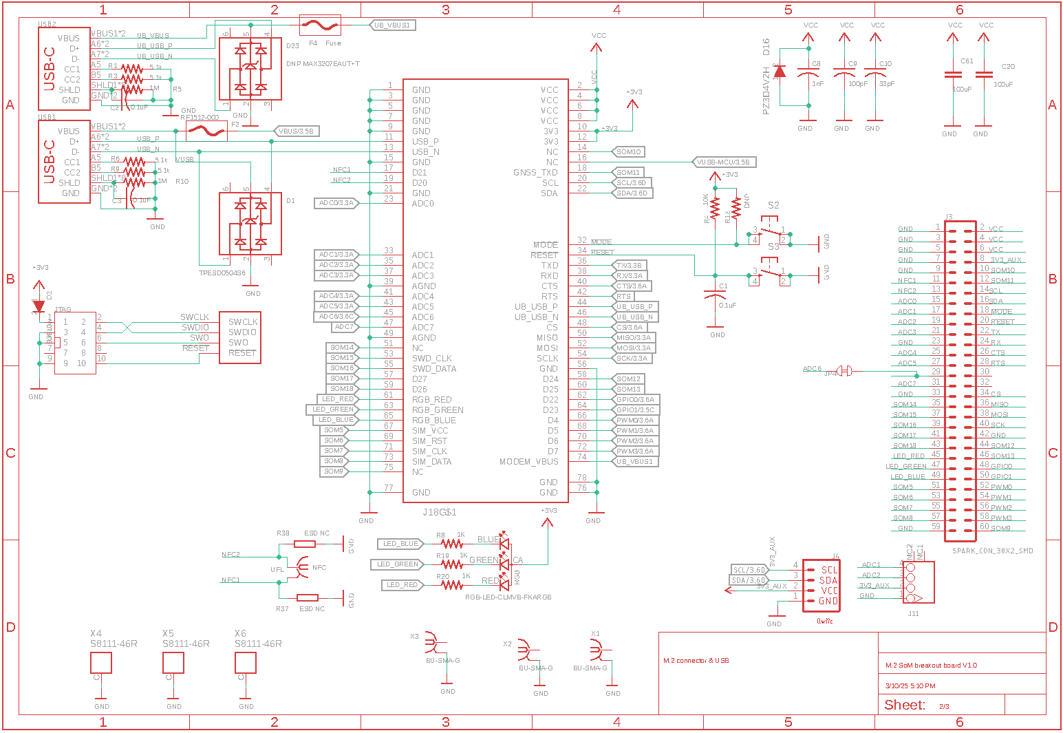
Page 2 - Schematics
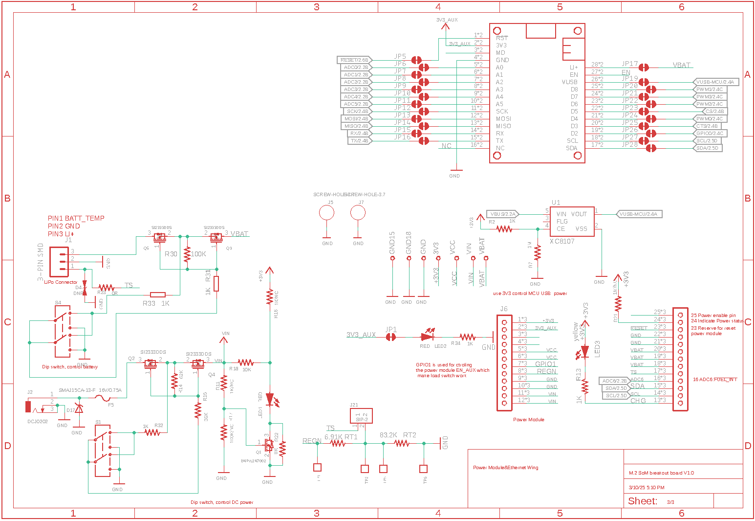
Page 3 - Schematics
Mechanical specifications
| Parameter | Value |
|---|---|
| Operating temperature | -20°C to 65°C |
Dimensions and weight
| Parameter | Value | Unit |
|---|---|---|
| Dimensions | 140 × 122 | millimeters (mm) |
| Weight | 125 | grams (g) |
- Weight includes an M-SoM and PM-BAT power module
Certification documents
Battery information
- 1-cell 3100 mAh battery pack (manufacturer datasheet)
- Battery cell (manufacturer datasheet for cells in the battery packs)
- This is the same battery as the 1-cell Tachyon battery pack
Revision history
| Revision | Date | Author | Comments |
|---|---|---|---|
| pre | 2024-03-18 | RK | Initial Release (based on board v0.2 20240315) |
| 2024-03-19 | RK | USB-C power limitations | |
| 2024-04-16 | RK | Description of TS jumper was backwards | |
| 1 | 2024-05-22 | RK | Public release |
| 2 | 2024-05-29 | RK | Descriptions for labels 1 and 3 were reversed |
| 3 | 2024-08-08 | RK | Input voltage is 5 - 12 VDC, not 24 |
| 4 | 2024-09-18 | RK | Add firmware settings |
| 5 | 2025-03-11 | RK | Add schematics and design files |